Click to expand full text
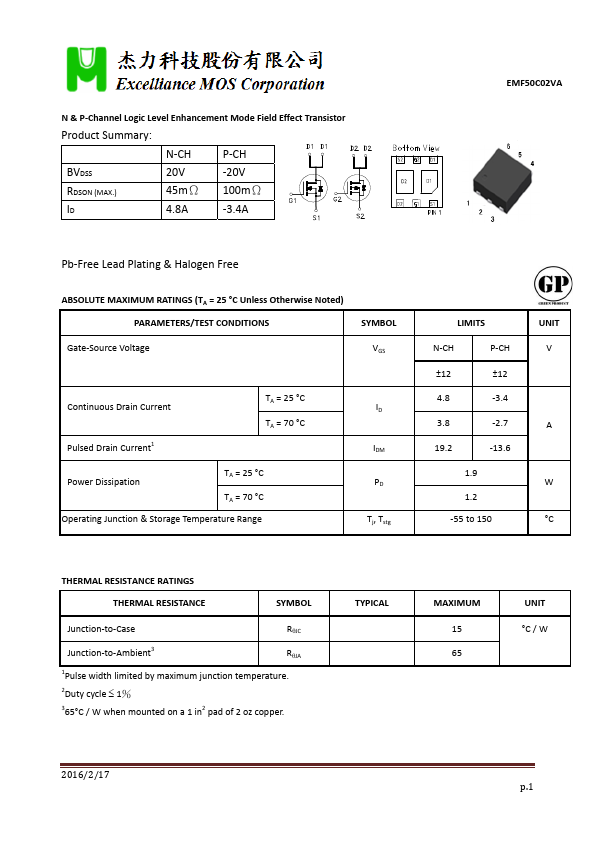
N & P‐Channel Logic Level Enhancement Mode Field Effect Transistor
Product Summary:
N‐CH
P‐CH
BVDSS
20V
‐20V
RDSON (MAX.)
45mΩ 100mΩ
ID
4.8A
‐3.4A
EMF50C02VA
Pb‐Free Lead Plating & Halogen Free
ABSOLUTE MAXIMUM RATINGS (TA = 25 °C Unless Otherwise Noted) PARAMETERS/TEST CONDITIONS
SYMBOL
Gate‐Source Voltage
VGS
Continuous Drain Current Pulsed Drain Current1
TA = 25 °C TA = 70 °C
Power Dissipation
TA = 25 °C TA = 70 °C
Operating Junction & Storage Temperature Range
ID IDM PD Tj, Tstg
LIMITS
N‐CH
P‐CH
±12
±12
4.8
‐3.4
3.8
‐2.7
19.2
‐13.6
1.9
1.2 ‐55 to 150
UNIT V
A W °C
THERMAL RESISTANCE RATINGS THERMAL RESISTANCE
SYMBOL
Junction‐to‐Case
RJC
Junction‐to‐Ambient3
RJA
1Pulse width limited by maximum junction temperature.
 EMF50C02VA Datasheet