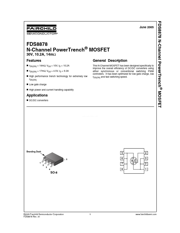
FDS8878
Features
- r DS(ON) = 14mΩ, VGS = 10V, ID = 10.2A
- r DS(ON) = 17mΩ, VGS = 4.5V, ID = 9.3A
- High performance trench technology for extremely low r DS(ON)
- Low gate charge
- High power and current handling capability
General Description
This N-Channel MOSFET has been designed specifically to improve the overall efficiency of DC/DC converters using either synchronous or conventional switching PWM controllers. It has been optimized for low gate charge, low r DS(ON) and fast switching speed.
Applications
- DC/DC converters
..
Branding Dash
4 3 2 1
6 7
1 2 3 4
SO-8
©2005 Fairchild Semiconductor Corporation FDS8878 Rev. A1
.fairchildsemi.
FDS8878 N-Channel Power Trench® MOSFET
MOSFET Maximum Ratings TA = 25°C unless otherwise noted
Symbol VDSS VGS Parameter Drain to Source Voltage Gate to Source Voltage Drain Current ID Continuous (TA = 25o C, VGS = 10V, Rθ JA = 50o C/W) Continuous (TA = Pulsed EAS PD TJ, TSTG Single Pulse Avalanche Energy (Note 1) Power dissipation Derate...