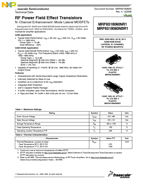
Datasheet4U Logo Datasheet4U.com

MRF6S18060NR1 - RF Power Field Effect Transistors

This page provides the datasheet information for the MRF6S18060NR1, a member of the MRF6S18060NBR1 RF Power Field Effect Transistors family.

Datasheet Summary

Features

  • Characterized with Series Equivalent Large - Signal Impedance Parameters.
  • Internally Matched for Ease of Use.
  • Qualified Up to a Maximum of 32 VDD Operation.
  • Integrated ESD Protection.
  • 225°C Capable Plastic Package.
  • N Suffix Indicates Lead - Free Terminations. RoHS Compliant.
  • In Tape and Reel. R1 Suffix = 500 Units per 44 mm, 13 inch Reel. Document Number: MRF6S18060N Rev. 4, 12/2008 MRF6S18060NR1 MRF6S18060NBR1 1800- 2000 MHz, 60.

📥 Download Datasheet

Datasheet preview – MRF6S18060NR1

Datasheet Details

Part number MRF6S18060NR1
Manufacturer Freescale Semiconductor
File Size 837.87 KB
Description RF Power Field Effect Transistors
Datasheet download datasheet MRF6S18060NR1 Datasheet
Additional preview pages of the MRF6S18060NR1 datasheet.
Other Datasheets by Freescale Semiconductor

Full PDF Text Transcription

Click to expand full text
Freescale Semiconductor Technical Data RF Power Field Effect Transistors N - Channel Enhancement - Mode Lateral MOSFETs Designed for GSM and GSM EDGE base station applications with frequencies from 1800 to 2000 MHz. Suitable for TDMA, CDMA, and multicarrier amplifier applications. GSM Application • Typical GSM Performance: VDD = 26 Vdc, IDQ = 600 mA, Pout = 60 Watts CW, f = 1990 MHz Power Gain — 15 dB Drain Efficiency - 50% GSM EDGE Application • Typical GSM EDGE Performance: VDD = 26 Volts, IDQ = 450 mA, Pout = 25 Watts Avg., Full Frequency Band (1805- 1880 MHz or 1930- 1990 MHz) Power Gain — 15.
Published: |