Click to expand full text
Freescale Semiconductor Technical Data
Document Number: MW7IC18100N Rev. 1, 6/2007
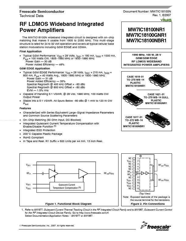
RF LDMOS Wideband Integrated Power Amplifiers
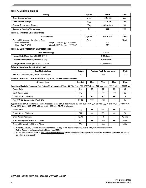
The MW7IC18100N wideband integrated circuit is designed with on - chip matching that makes it usable from 1805 to 2050 MHz. This multi - stage structure is rated for 24 to 32 Volt operation and covers all typical cellular base station modulations including GSM EDGE and CDMA. Final Application • Typical GSM Performance: VDD = 28 Volts, IDQ1 = 180 mA, IDQ2 = 1000 mA, Pout = 100 Watts CW, 1805 - 1880 MHz or 1930 - 1990 MHz Power Gain — 30 dB Power Added Efficiency — 48% GSM EDGE Application • Typical GSM EDGE Performance: VDD = 28 Volts, IDQ1 = 215 mA, IDQ2 = 800 mA, Pout = 40 Watts Avg.
 MW7IC18100NBR1 Datasheet