Click to expand full text
HD74AC00
Quad 2-Input NAND Gate
Feature
• Outputs Source/Sink 24 mA
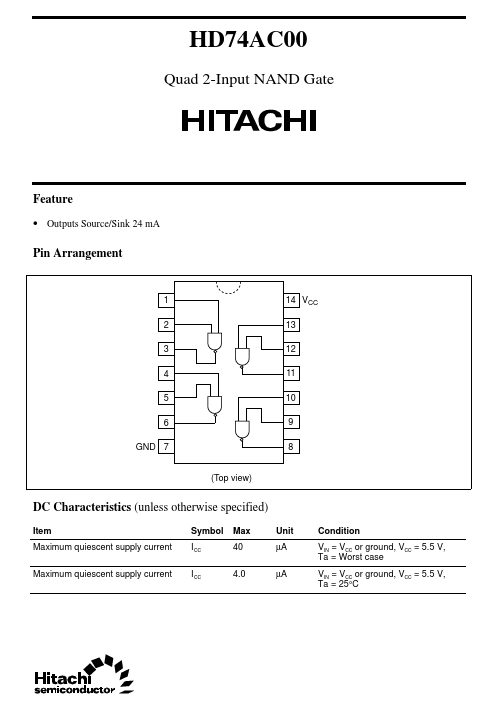
Pin Arrangement
1 2 3 4 5 6 GND 7 (Top view)
14 VCC 13 12 11 10 9 8
DC Characteristics (unless otherwise specified)
Item Maximum quiescent supply current Maximum quiescent supply current Symbol I CC I CC Max 40 4.0 Unit µA µA Condition VIN = VCC or ground, VCC = 5.5 V, Ta = Worst case VIN = VCC or ground, VCC = 5.5 V, Ta = 25°C
HD74AC00
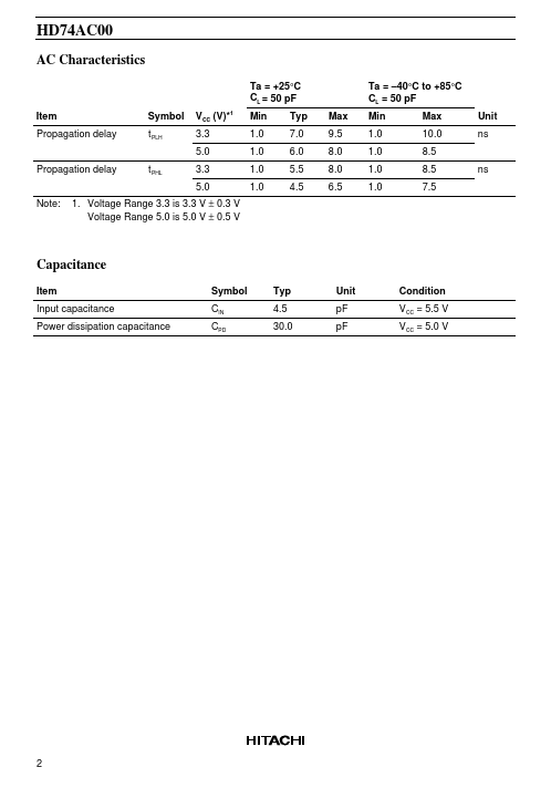
AC Characteristics
Ta = +25°C CL = 50 pF Item Propagation delay Symbol t PLH VCC (V)*1 3.3 5.0 Propagation delay t PHL 3.3 5.0 Note: 1. Voltage Range 3.3 is 3.3 V ± 0.3 V Voltage Range 5.0 is 5.0 V ± 0.5 V Min 1.0 1.0 1.0 1.0 Typ 7.0 6.0 5.5 4.5 Max 9.5 8.0 8.0 6.5 Ta = –40°C to +85°C CL = 50 pF Min 1.0 1.0 1.0 1.0 Max 10.0 8.5 8.5 7.
 HD74AC00 Datasheet