Datasheet Details
| Part number | HD74ALVCH162835 |
|---|---|
| Manufacturer | Hitachi Semiconductor |
| File Size | 53.11 KB |
| Description | 18-bit Universal Bus Drivers with 3-state Outputs |
| Datasheet |
 HD74ALVCH162835 Datasheet HD74ALVCH162835 Datasheet
|
|
|
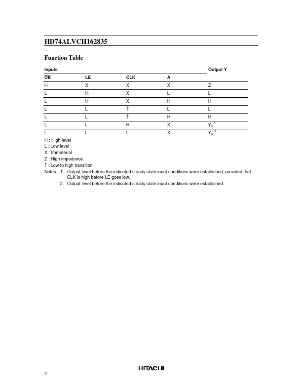
Data flow from A to Y is controlled by the output enable (OE ).
The device operates in the transparent mode when LE is high.
The A data is latched if CLK is held at a high or low logic level.
| Part number | HD74ALVCH162835 |
|---|---|
| Manufacturer | Hitachi Semiconductor |
| File Size | 53.11 KB |
| Description | 18-bit Universal Bus Drivers with 3-state Outputs |
| Datasheet |
HD74ALVCH162835 Datasheet
|
|
|
|