Datasheet Details
| Part number | HD74ALVCH16820 |
|---|---|
| Manufacturer | Hitachi Semiconductor |
| File Size | 51.05 KB |
| Description | 3.3-V 10-bit Flip Flops with Dual Outputs |
| Datasheet |
 HD74ALVCH16820 Datasheet HD74ALVCH16820 Datasheet
|
|
|
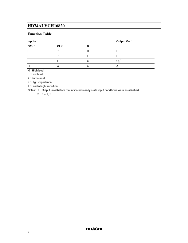
The flip flops of the HD74ALVCH16820 are edge triggered D-type flip flops.
On the positive transition of the clock (CLK) input, the device provides true data at the Q outputs.
| Part number | HD74ALVCH16820 |
|---|---|
| Manufacturer | Hitachi Semiconductor |
| File Size | 51.05 KB |
| Description | 3.3-V 10-bit Flip Flops with Dual Outputs |
| Datasheet |
HD74ALVCH16820 Datasheet
|
|
|
|