Datasheet Details
| Part number | HD74HC651 |
|---|---|
| Manufacturer | Hitachi Semiconductor |
| File Size | 55.45 KB |
| Description | Octal Bus Transceivers/Registers |
| Datasheet |
 HD74HC651 Datasheet HD74HC651 Datasheet
|
|
|
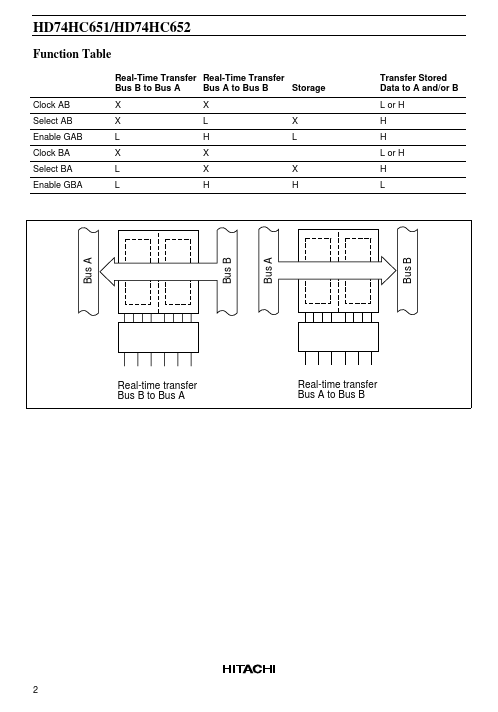
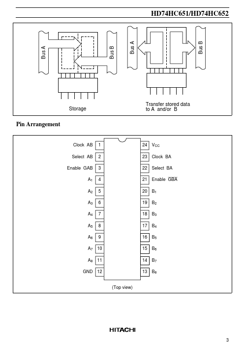
This device consists of bus transceiver circuits, D-type flip-flops, and control circuitry arranged for multiplexed transmission of data directly from the data bus or from the internal storage registers.
Enable GAB and GBA are provided to cotrol the transceiver functions.
| Part number | HD74HC651 |
|---|---|
| Manufacturer | Hitachi Semiconductor |
| File Size | 55.45 KB |
| Description | Octal Bus Transceivers/Registers |
| Datasheet |
HD74HC651 Datasheet
|
|
|
|