Datasheet Details
| Part number | 74HC595 |
|---|---|
| Manufacturer | Hitachi |
| File Size | 57.87 KB |
| Description | 8-bit Shift Register/Latch |
| Datasheet |
 74HC595 Datasheet 74HC595 Datasheet
|
|
|
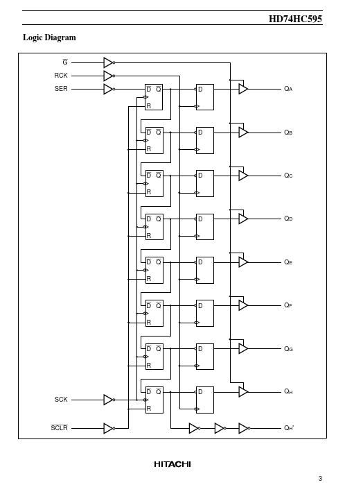
This device each contains an 8-bit serial-in, parallel-out shift register that feeds an 8-bit D-type storage register.
The storage register has parallel 3-state outputs.
Separate clocks are provided for both the shift register and the storage register.
| Part number | 74HC595 |
|---|---|
| Manufacturer | Hitachi |
| File Size | 57.87 KB |
| Description | 8-bit Shift Register/Latch |
| Datasheet |
74HC595 Datasheet
|
|
|
|