Datasheet Details
- Part number
- HY5V52F
- Manufacturer
- Hynix Semiconductor
- File Size
- 345.39 KB
- Datasheet
- HY5V52F_HynixSemiconductor.pdf
- Description
- 4Banks x 2M x 32bits Synchronous DRAM
HY5V52F Description
www.DataSheet4U.com Preliminary HY5V52(L)F(P) Series 4Banks x 2M x 32bits Synchronous DRAM Document Title 4Bank x 2M x 32bits Synchronous DRAM Revis.HY5V52F Features
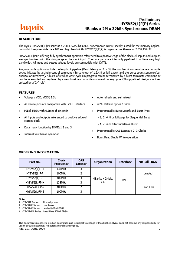
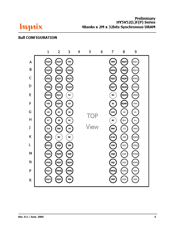
* Voltage : VDD, VDDQ 3.3V All device pins are compatible with LVTTL interface 90Ball FBGA with 0.8mm of pin pitch All inputs and outputs referenced to positive edge of system clock Data mask function by DQM0,1,2 and 3HY5V52F Applications
* which require wide data I/O and high bandwidth. HY5V52(L)F(P) is organized as 4banks of 2,097,152x32. HY5V52(L)F(P) is offering fully synchronous operation referenced to a positive edge of the clock. All inputs and outputs are synchronized with the rising edge of the clock input. The data paths are
📁 Related Datasheet
📌 All Tags