Datasheet4U Logo Datasheet4U.com

ICS9DB102 Datasheet - IDT

ICS9DB102 - Two Output Differential Buffer

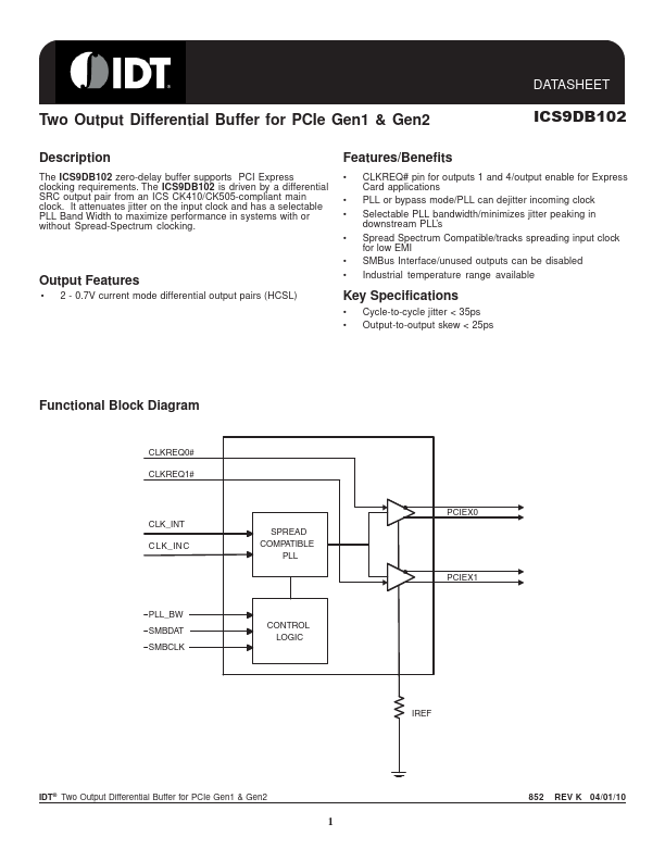
The ICS9DB102 zero-delay buffer supports PCI Express clocking requirements. The ICS9DB102 is driven by a differential SRC output pair from an ICS CK410/CK505-compliant main clock. It attenuates jitter on the input clock and has a selectable PLL Band Width to maximize performance in systems with or w.

ICS9DB102 Features

* 2 - 0.7V current mode differential output pairs (HCSL) Features/Benefits

* CLKREQ# pin for outputs 1 and 4/output enable for Express Card applications

* PLL or bypass mode/PLL can dejitter incoming clock

* Selectable PLL bandwidth/minimizes jitter peaking in downst

ICS9DB102-IDT.pdf

Preview of ICS9DB102 PDF
ICS9DB102 Datasheet Preview Page 2 ICS9DB102 Datasheet Preview Page 3

Datasheet Details

Part number:

ICS9DB102

Manufacturer:

IDT

File Size:

182.70 KB

Description:

Two output differential buffer.

ICS9DB102 Distributor

📁 Related Datasheet

📌 All Tags