Datasheet Details
| Part number | ICS9DB106 |
|---|---|
| Manufacturer | Integrated Circuit Systems |
| File Size | 263.96 KB |
| Description | 6 Output PCI Express Buffer |
| Datasheet |
 ICS9DB106 Datasheet ICS9DB106 Datasheet
|
|
|
| Part number | ICS9DB106 |
|---|---|
| Manufacturer | Integrated Circuit Systems |
| File Size | 263.96 KB |
| Description | 6 Output PCI Express Buffer |
| Datasheet |
ICS9DB106 Datasheet
|
|
|
|
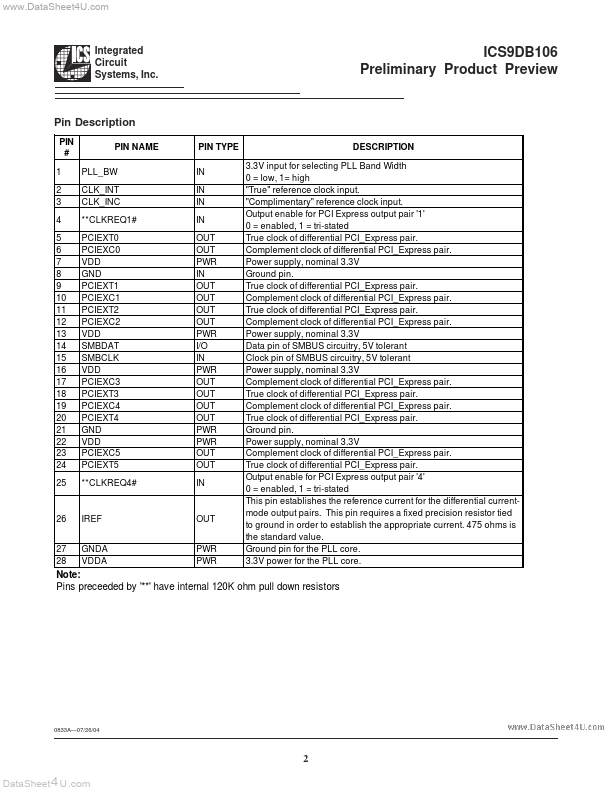
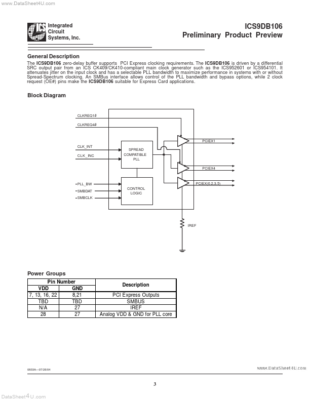
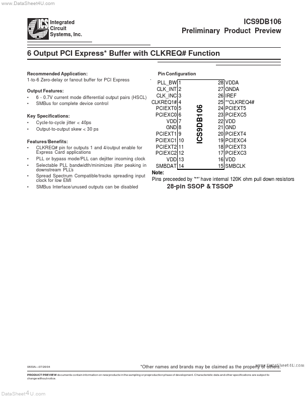
PIN # 1 2 3 4 5 6 7 8 9 10 11 12 13 14 15 16 17 18 19 20 21 22 23 24 25 PIN NAME PLL_BW CLK_INT CLK_INC CLKREQ1# PCIEXT0 PCIEXC0 VDD GND PCIEXT1 PCIEXC1 PCIEXT2 PCIEXC2 VDD SMBDAT SMBCLK VDD PCIEXC3 PCIEXT3 PCIEXC4 PCIEXT4 GND VDD PCIEXC5 PCIEXT5 CLKREQ4# PIN TYPE IN IN IN IN OUT OUT PWR IN OUT OUT OUT OUT PWR I/O IN PWR OUT OUT OUT OUT PWR PWR OUT OUT IN DESCRIPTION 3.3V input for selecting PLL Band Width 0 = low, 1= high "True" reference clock input.
📁 Similar Datasheet