Datasheet4U Logo Datasheet4U.com

ICS9DBL411A Datasheet - Renesas

ICS9DBL411A Four Output Differential Fanout Buffer

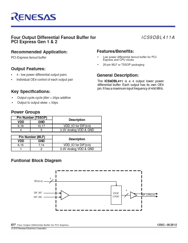
The ICS9DBL411 is a 4 output lower power differential buffer. Each output has its own OE# pin. It has a maximum input frequency of 400 MHz. Power Groups Pin Number (TSSOP) VDD GND 9,18 10,17 45 Pin Number (MLF) VDD GND 6,15 7,14 12 Description VDD_IO for DIF(3:0) 3.3V Analog VDD & GND D.

ICS9DBL411A Features

* 4 - low power differential output pairs

* Individual OE# control of each output pair Key Specifications:

* Output cycle-cycle jitter < 25ps additive

* Output to output skew: < 50ps Features/Benefits:

* Low power differential fanout buffer for PCIExpress an

ICS9DBL411A Datasheet (189.86 KB)

Preview of ICS9DBL411A PDF
ICS9DBL411A Datasheet Preview Page 2 ICS9DBL411A Datasheet Preview Page 3

Datasheet Details

Part number:

ICS9DBL411A

Manufacturer:

Renesas ↗

File Size:

189.86 KB

Description:

Four output differential fanout buffer.

📁 Related Datasheet

ICS9DBL411 Four Output Differential Fanout Buffer (IDT)

ICS9DB102 Two Output Differential Buffer (IDT)

ICS9DB102 2 Output PCI Express Buffer (Integrated Circuit Systems)

ICS9DB102 Two Output Differential Buffer (Renesas)

ICS9DB104 Four Output Differential Buffer (Integrated Circuit Systems)

ICS9DB104 Four Output Differential Buffer (Renesas)

ICS9DB106 6 Output PCI Express Buffer (Integrated Circuit Systems)

ICS9DB108 Eight Output Differential Buffer (Integrated Circuit Systems)

TAGS

ICS9DBL411A Four Output Differential Fanout Buffer Renesas

ICS9DBL411A Distributor