Datasheet Details
| Part number | SSTE32882KA1 |
|---|---|
| Manufacturer | IDT |
| File Size | 1.17 MB |
| Description | 1.25V/1.35V/1.5V REGISTERING CLOCK DRIVER |
| Datasheet |
 SSTE32882KA1-IDT.pdf SSTE32882KA1-IDT.pdf
|
|
|
The SSTE32882KA1 by IDT is a 1.25V/1.35V/1.5V REGISTERING CLOCK DRIVER. Below is the official datasheet preview.
| Part number | SSTE32882KA1 |
|---|---|
| Manufacturer | IDT |
| File Size | 1.17 MB |
| Description | 1.25V/1.35V/1.5V REGISTERING CLOCK DRIVER |
| Datasheet |
SSTE32882KA1-IDT.pdf
|
|
|
|
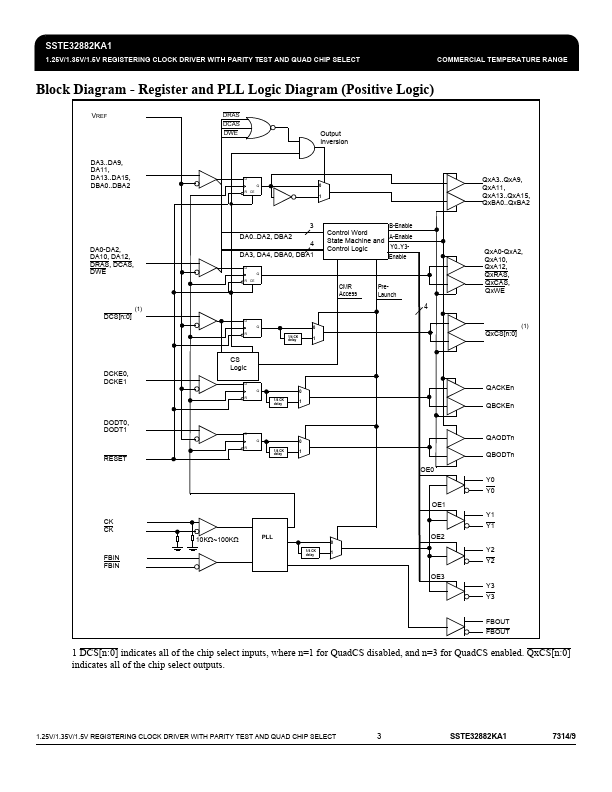
This 28-bit 1:2, or 26-bit 1:2 and 4-bit 1:1, registering clock driver with parity is designed for 1.25V, 1.35V and 1.5V VDD operation.
📁 SSTE32882KA1 Similar Datasheet