Description
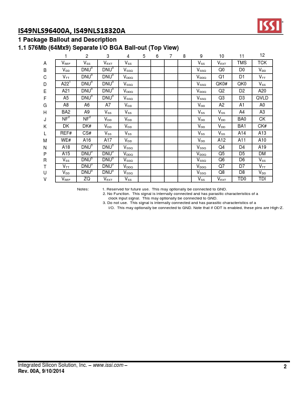
1.1 576Mb (64Mx9) Separate I/O BGA Ball-out (Top View)
1 2 3 4 5678
A
VREF
VSS
VEXT
VSS
B
VDD
DNU3
DNU3
VSSQ
C
VTT
DNU3
DNU3
VDDQ
D
A221
DNU3 DNU3
VSSQ
E
A21
DNU3
DNU3
VDDQ
F
A5
DNU3
DNU3
VSSQ
G A8 A6 A7 VDD
H
BA2 A9
VSS
VSS
J
NF2
NF2
VDD
VDD
K DK DK# VDD VDD
L REF# CS# VSS VSS
M
WE#
A16
A17
VDD
N
A18
DNU3
DNU3
VSSQ
P
A15
DNU3
DNU3
VDDQ
R
VSS
DNU3
DNU3
VSSQ
T
VTT
DNU3
DNU3
VDDQ
U
VDD
DNU3
DNU3
VSSQ
V
VREF
ZQ
VEXT
VSS
Features
- 533MHz DDR operation (1.067 Gb/s/pin data rate).
- 38.4Gb/s peak bandwidth (x18 at 533 MHz clock
frequency).
- Reduced cycle time (15ns at 533MHz).
- 32ms refresh (16K refresh for each bank; 128K
refresh command must be issued in total each 32ms).
- 8 internal banks.
- Non-multiplexed addresses (address multiplexing option available).
- SRAM-type interface.
- Programmable READ latency (RL), row cycle time, and burst sequence length.
- Balanced READ and WRITE latenci.
 IS49NLS96400A-IntegratedSiliconSolution.pdf