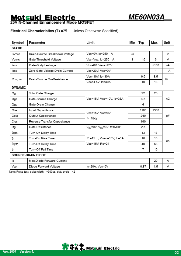
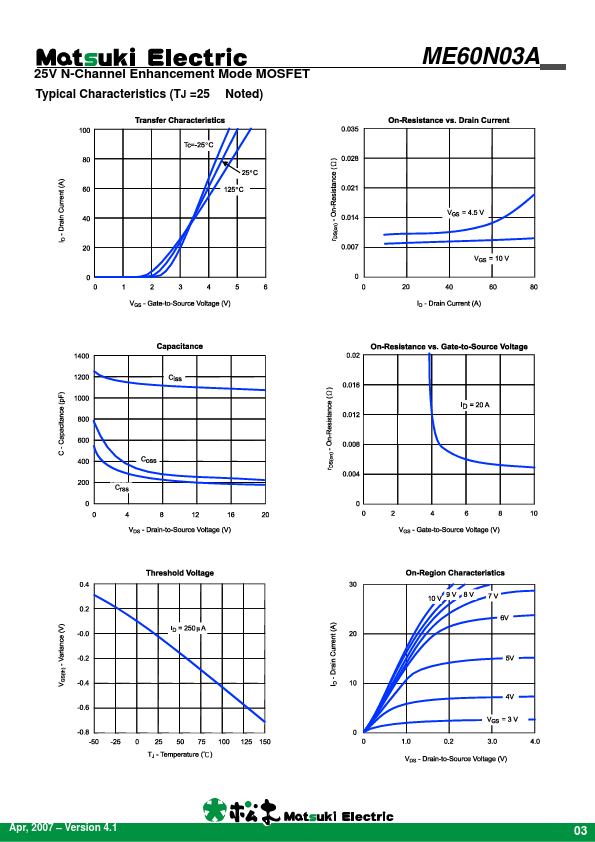
Click to expand full text
25V N-Channel Enhancement Mode MOSFET
VDS=25V RDS(ON), Vgs@10V,Ids@30A = 8.5m RDS(ON), Vgs@4.5V,Ids@30A =13m
ME60N03A
FEATURES
Advanced trench process technology High density cell design for ultra low on-resistance Specially designed for DC/DC converters and motor drivers Fully characterized avalanche voltage and current
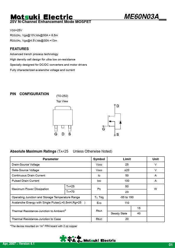
PIN
CONFIGURATION
(TO-252) Top View
Absolute Maximum Ratings (TA=25
Parameter
Drain-Source Voltage Gate-Source Voltage Continuous Drain Current Pulsed Drain Current Maximum Power Dissipation
Unless Otherwise Noted)
Symbol
VDSS VGSS ID IDM
Limit
25 ±20 50 100 50 23 -55 to 150 110 15 Steady State 20 40
Unit
V V A A W
TA=25 TA=70
PD TJ, Tstg ) EAS RθJA RθJC
Operating Junction and Storage Temperature Range Avalanche Energy with Single Pulse(L=0.
 ME60N03A Datasheet