Datasheet4U Logo Datasheet4U.com

MTP3N50E - TMOS POWER FET

Datasheet Summary

Features

  • Device stresses increase with commutation speed, so tfrr is specified with a minimum value. Faster commutation speeds require an appropriate derating of IFM, peak VR or both. Ultimately, tfrr is limited primarily by device, package, and circuit impedances. Maximum device stress occurs during trr as the diode goes from conduction to reverse blocking. VDS(pk) is the peak drain.
  • to.
  • source voltage that the device must sustain during commutation; IFM is the maximum forward source-drai.

📥 Download Datasheet

Datasheet preview – MTP3N50E

Datasheet Details

Part number MTP3N50E
Manufacturer Motorola
File Size 251.88 KB
Description TMOS POWER FET
Datasheet download datasheet MTP3N50E Datasheet
Additional preview pages of the MTP3N50E datasheet.
Other Datasheets by Motorola

Full PDF Text Transcription

Click to expand full text
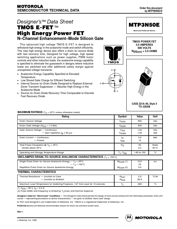
MOTOROLA SEMICONDUCTOR TECHNICAL DATA Order this document by MTP3N50E/D ™ Data Sheet TMOS E-FET.™ High Energy Power FET Designer's MTP3N50E Motorola Preferred Device N–Channel Enhancement–Mode Silicon Gate This advanced high voltage TMOS E–FET is designed to withstand high energy in the avalanche mode and switch efficiently. This new high energy device also offers a drain–to–source diode with fast recovery time. Designed for high voltage, high speed switching applications such as power supplies, PWM motor controls and other inductive loads, the avalanche energy capability is specified to eliminate the guesswork in designs where inductive loads are switched and offer additional safety margin against unexpected voltage transients.
Published: |