Click to expand full text
MOTOROLA
SEMICONDUCTOR TECHNICAL DATA
Order this document by MTV25N50E/D
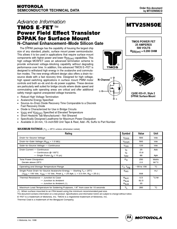
Advance Information
TMOS E-FET.™ Power Field Effect Transistor D3PAK for Surface Mount
The D3PAK package has the capability of housing the largest chip size of any standard, plastic, surface mount power semiconductor. This allows it to be used in applications that require surface mount components with higher power and lower RDS(on) capabilities. This high voltage MOSFET uses an advanced termination scheme to provide enhanced voltage–blocking capability without degrading performance over time. In addition, this advanced TMOS E–FET is designed to withstand high energy in the avalanche and commutation modes. The new energy efficient design also offers a drain–to– source diode with a fast recovery time.
 MTV25N50E Datasheet