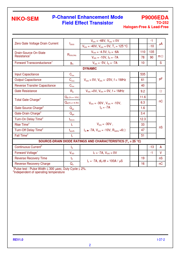
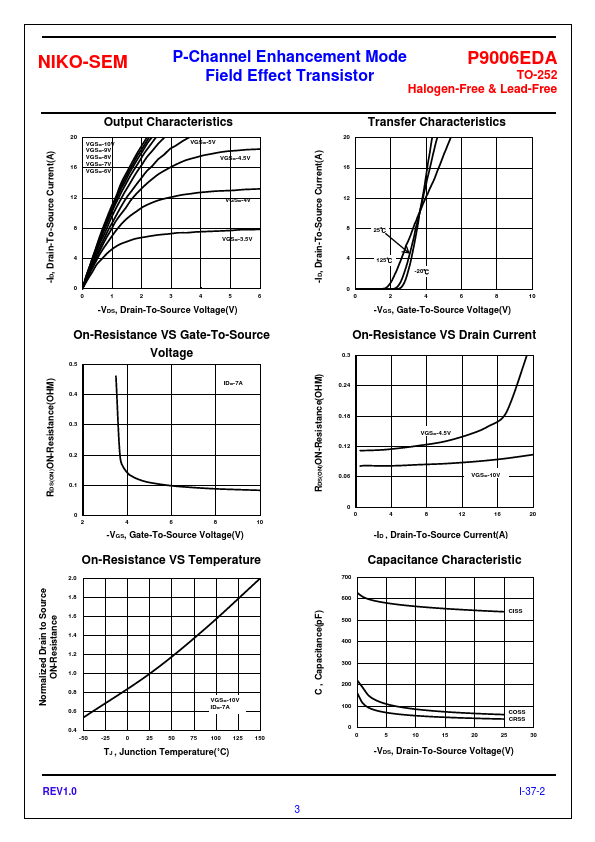
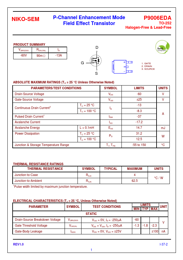
Datasheet4U Logo Datasheet4U.com

P9006EDA - P-Channel Enhancement Mode Field Effect Transistor

This page provides the datasheet information for the P9006EDA, a member of the P9006EDA-NIKO P-Channel Enhancement Mode Field Effect Transistor family.

📥 Download Datasheet

Datasheet preview – P9006EDA

Datasheet Details

Part number P9006EDA
Manufacturer NIKO-SEM
File Size 210.83 KB
Description P-Channel Enhancement Mode Field Effect Transistor
Datasheet download datasheet P9006EDA Datasheet
Additional preview pages of the P9006EDA datasheet.
Other Datasheets by NIKO-SEM

Full PDF Text Transcription

Click to expand full text
NIKO-SEM P-Channel Enhancement Mode P9006EDA Field Effect Transistor TO-252 Halogen-Free & Lead-Free PRODUCT SUMMARY V(BR)DSS RDS(ON) -60V 90mΩ ID -13A D G S ABSOLUTE MAXIMUM RATINGS (TA = 25 °C Unless Otherwise Noted) PARAMETERS/TEST CONDITIONS SYMBOL Drain-Source Voltage Gate-Source Voltage Continuous Drain Current2 Pulsed Drain Current1 Avalanche Current Avalanche Energy Power Dissipation Junction & Storage Temperature Range TC = 25 °C TC = 100 °C L = 0.1mH TC = 25 °C TC = 100 °C VDS VGS ID IDM IAS EAS PD TJ, Tstg 1. GATE 2. DRAIN 3. SOURCE LIMITS -60 ±25 -13 -8.3 -37 -17.2 14.7 31.2 12.
Published: |