Description
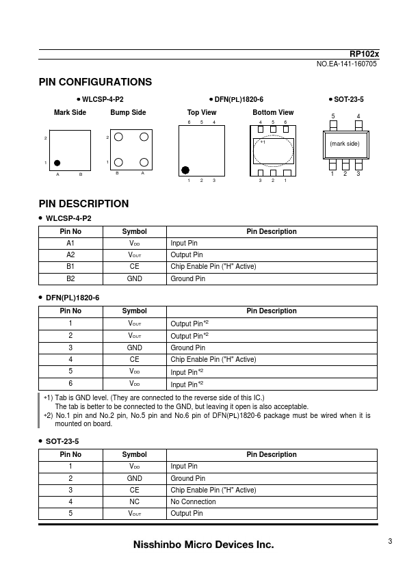
WLCSP-4-P2
Pin No A1 A2 B1 B2
Symbol VDD VOUT CE GND
Pin Description Input Pin Output Pin Chip Enable Pin ("H" Active) Ground Pin
DFN(PL)1820-6
Pin No 1 2
Symbol VOUT VOUT
Output Pin2 Output Pin2
Pin Description
3
GND
Ground Pin
4
CE
Chip Enable Pin ("H" Active)
5
VDD
Input Pin2
6
VDD
Input Pin2
∗1) Tab is GND level.(They are connected to the reverse side of this IC.)
The tab is better to be connected to the GND, but leaving it open is also acceptable
Features
- Supply Current Typ. 50A.
- Standby Mode Typ. 0.1A.
- Dropout Voltage Typ. 0.12V (IOUT300mA, VOUT2.8V).
- Ripple Rejection Typ. 80dB (f1kHz).
- Temperature-Drift Coefficient of Output Voltage Typ. ±20ppm/C.
- Line Regulation Typ. 0.02%/V.
- Output Voltage Accuracy0.8%.
- Packages WLCSP-4-P2, DFN(PL)1820-6, SOT-23-5.
- Input Voltage Range 1.7V to 5.25V.
- Output Voltage Range1.2V to 3.3V (0.1V steps)
(For other voltages, please refer to MARK.
 RP102N Datasheet