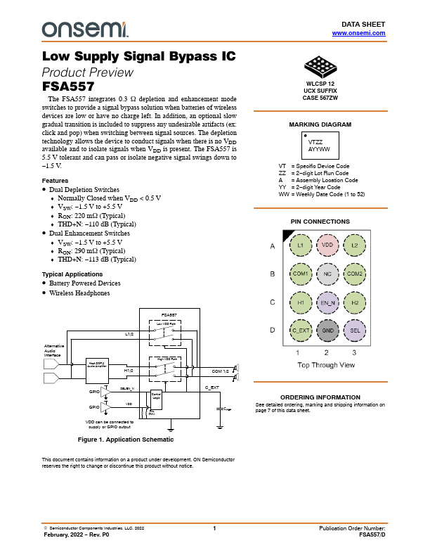
Datasheet Details
| Part number | FSA557 |
|---|---|
| Manufacturer | ON Semiconductor ↗ |
| File Size | 203.99 KB |
| Description | Low Supply Signal Bypass-IC |
| Datasheet |
 FSA557-ONSemiconductor.pdf FSA557-ONSemiconductor.pdf
|
| Part number | FSA557 |
|---|---|
| Manufacturer | ON Semiconductor ↗ |
| File Size | 203.99 KB |
| Description | Low Supply Signal Bypass-IC |
| Datasheet |
FSA557-ONSemiconductor.pdf
|
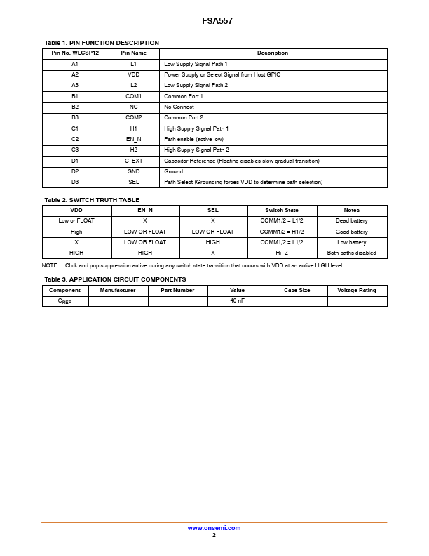
Pin No.
📁 FSA557 Similar Datasheet