NB6L11S - Input to LVDS Fanout Buffer/Translator
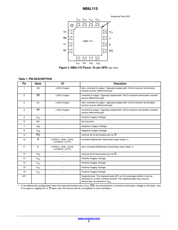
Pin Name I/O Description 1 Q0 LVDS Output Non *inverted D output. Typically loaded with 100 W receiver termination resistor across differential pair. 2 Q0 LVDS Output Inverted D output. Typically loaded with 100 W receiver termination resistor across differential pair. 3 Q1 LVD.
NB6L11S VOLTAGE (130 mV/div) 2.5 V 1:2 AnyLevel] Input to LVDS Fanout Buffer / Translator The NB6L11S is a differential 1:2 clock or data receiver and will accept AnyLevelâ„¢ input signals: LVPECL, CML, LVCMOS, LVTTL, or LVDS. These signals will be translated to LVDS and two identical copies of Clock or Data will be distributed, operating up to 2.0 GHz or 2.5 Gb/s, respectively. As such, the NB6L11S is ideal for SONET, GigE, Fiber Channel, Backplane and other Clock or Data distribution applicati.
NB6L11S Features
* Input Clock Frequency > 2.0 GHz
* Input Data Rate > 2.5 Gb/s
* RMS Clock Jitter
* 0.5 ps, Typical
* 622 Mb/s Data Dependent Jitter
* 6 ps, Typical
* 380 ps Typical Propagation Delay
* 120 ps Typical Rise and Fall Times
* Single