Description
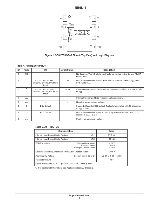
Pin 1 2 Name NC D I/O
LVDS, CML, LVPECL, LVNECL, LVTTL, LVCMOS Input LVDS, CML, LVPECL, LVNECL, LVTTL, LVCMOS Input
ECL Output ECL Output
Default State
LOW Description No Connect.
inverted differential clock/data input.
Features
- perature range. Functional operation of the device exceeding these conditions is not implied. Device specification limit values are applied individually under normal operating conditions and not valid simultaneously. 8. Vth is applied to the complementary input when operating in single.
- ended mode. 9. VCMR minimum varies 1:1 with VEE, VCMR maximum varies 1:1 with VCC. 10. Input and output parameters vary 1:1 with VCC. VEE can vary +0.925 V to.
- 0.5 V. 11. All input and output pins.
 NB6L16_ONSemiconductor.pdf