Datasheet Details
| Part number | NB6N11S |
|---|---|
| Manufacturer | ON Semiconductor |
| File Size | 314.24 KB |
| Description | Input to LVDS Fanout Buffer/Translator |
| Datasheet |
 NB6N11S_ONSemiconductor.pdf NB6N11S_ONSemiconductor.pdf
|
|
|
The NB6N11S by ON Semiconductor is a Input to LVDS Fanout Buffer/Translator. Below is the official datasheet preview.
| Part number | NB6N11S |
|---|---|
| Manufacturer | ON Semiconductor |
| File Size | 314.24 KB |
| Description | Input to LVDS Fanout Buffer/Translator |
| Datasheet |
NB6N11S_ONSemiconductor.pdf
|
|
|
|
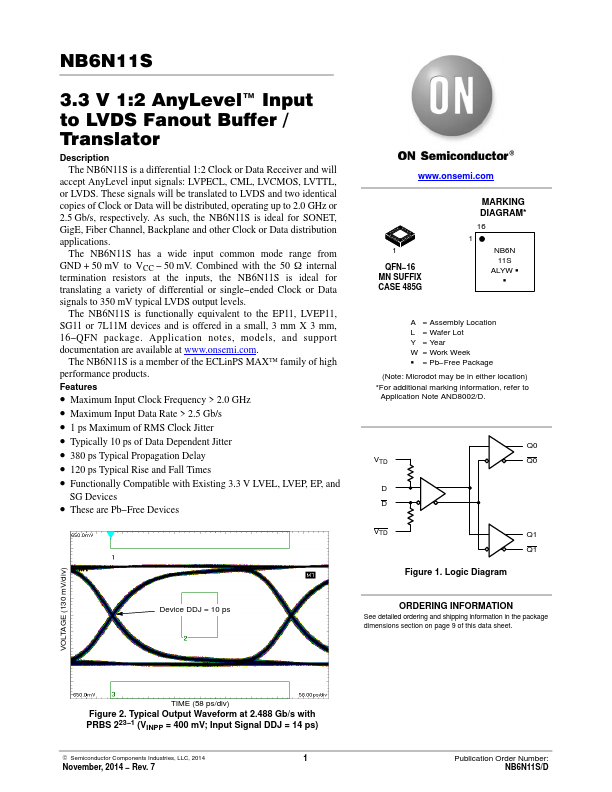
The NB6N11S is a differential 1:2 Clock or Data Receiver and will accept AnyLevel input signals: LVPECL, CML, LVCMOS, LVTTL, or LVDS.These signals will be translated to LVDS and two identical copies of Clock or Data will be distributed, operating up to 2.0 GHz or 2.5 Gb/s, respectively.As such, the NB6N11S is ideal for SONET, GigE, Fiber Channel, Backplane and other Clock or Data distribution applications.The NB6N11S has a wide input common mode range from GND + 50 mV to VCC 50 mV.
📁 NB6N11S Similar Datasheet