Datasheet Details
| Part number | NB6N14S |
|---|---|
| Manufacturer | ON Semiconductor |
| File Size | 367.51 KB |
| Description | Differential Input to LVDS Fanout Buffer/Translator |
| Datasheet |
 NB6N14S_ONSemiconductor.pdf NB6N14S_ONSemiconductor.pdf
|
|
|
The NB6N14S by ON Semiconductor is a Differential Input to LVDS Fanout Buffer/Translator. Below is the official datasheet preview.
| Part number | NB6N14S |
|---|---|
| Manufacturer | ON Semiconductor |
| File Size | 367.51 KB |
| Description | Differential Input to LVDS Fanout Buffer/Translator |
| Datasheet |
NB6N14S_ONSemiconductor.pdf
|
|
|
|
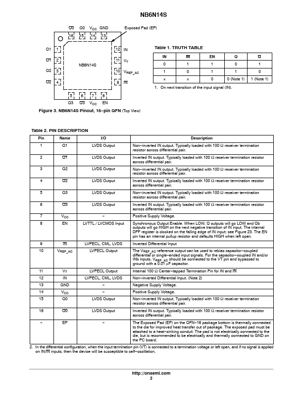
Pin Name I/O Description 1 Q1 LVDS Output Non inverted IN output. inverted IN output.
📁 NB6N14S Similar Datasheet