Datasheet Details
| Part number | NCP5211A |
|---|---|
| Manufacturer | ON Semiconductor |
| File Size | 148.66 KB |
| Description | Low Voltage Synchronous Buck Controller |
| Datasheet |
 NCP5211A Datasheet NCP5211A Datasheet
|
|
|
| Part number | NCP5211A |
|---|---|
| Manufacturer | ON Semiconductor |
| File Size | 148.66 KB |
| Description | Low Voltage Synchronous Buck Controller |
| Datasheet |
NCP5211A Datasheet
|
|
|
|
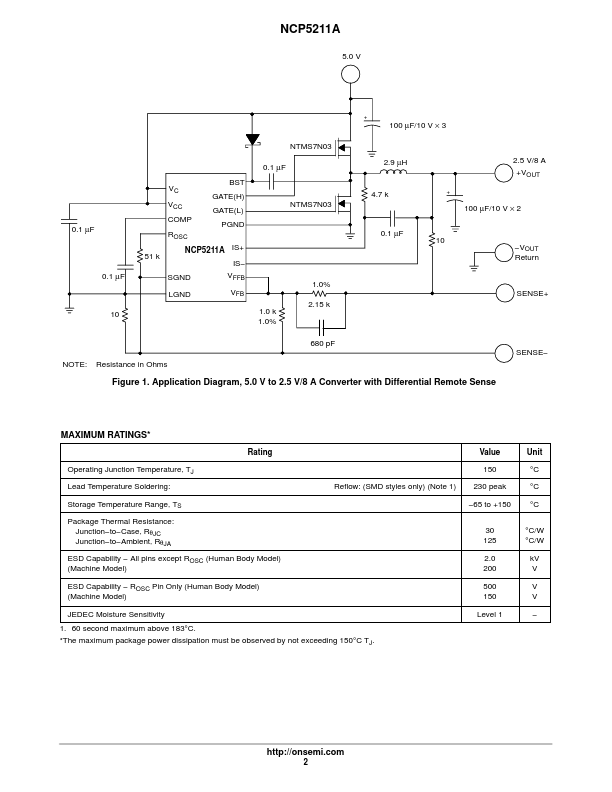
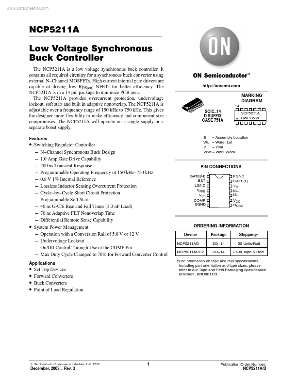
PIN NO. IS+ VC GATE(L) PGND FUNCTION High Side Switch FET driver pin.
📁 Similar Datasheet