Datasheet4U Logo Datasheet4U.com

MN3885S Datasheet - Panasonic Semiconductor

MN3885S_PanasonicSemiconductor.pdf
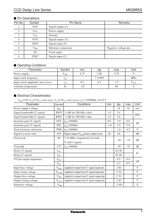
Preview of MN3885S PDF
MN3885S Datasheet Preview Page 2 MN3885S Datasheet Preview Page 3

Datasheet Details

Part number:

MN3885S

Manufacturer:

Panasonic Semiconductor

File Size:

52.71 KB

Description:

Ntsc-compatible ccd video signal delay element.

MN3885S, NTSC-Compatible CCD Video Signal Delay Element

Pin No.

1 2 3 4 5 6 7 8 Symbol VOC VDD VSS VOY VINY VBB XI VINC Pin Name Signal output (C) Power supply Ground Signal output (Y) Signal input (Y) Substrate connection Clock input Signal input (C) MN3885S Remarks Negative voltage pin Operating Conditions Parameter Power supply Input clock freque

CCD Delay Line Series MN3885S NTSC-Compatible CCD Video Signal Delay Element Overview The MN3885S is a CCD signal delay element for video signal processing applications.

It contains such components as a shift register clock driver, charge I/O blocks, two CCD delay elements, a clamp bias circuit, resampling output amplifiers, and booster circuits.

The MN3885S samples the input using the supplied clock signal with a frequency 7.15909 MHz of twice the NTSC color signal subcarrier frequency, and af

MN3885S Features

* Single 5.0 V power supply Single chip combining luminance signal delay line and delay line for color signal converted to the low frequency. Low EMI levels from clock during driving Applications VCRs, Video cameras Structure and Operation The MN3885S consists of the operational blocks shown in the

📁 Related Datasheet

📌 All Tags

Panasonic Semiconductor MN3885S-like datasheet