Click to expand full text
CCD Delay Line Series
MN3881S
PAL-Compatible CCD Video Signal Delay Element
Overview
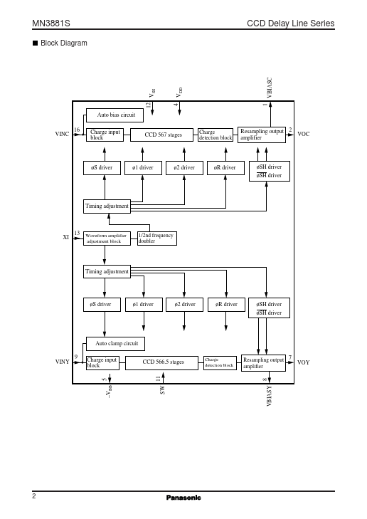
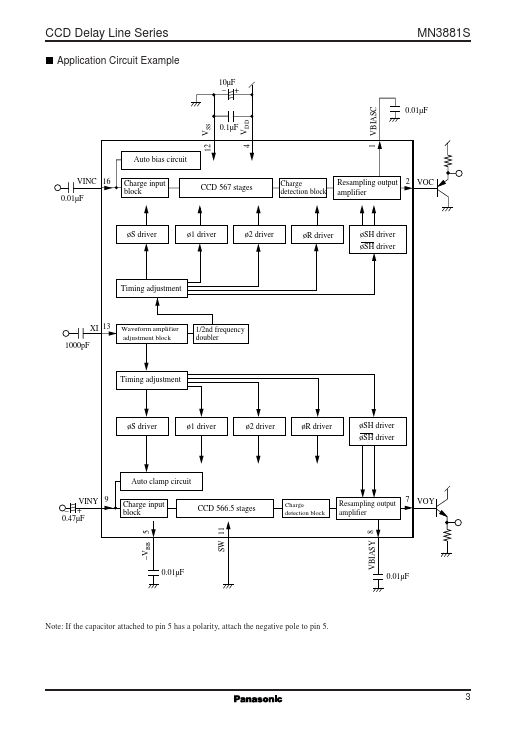
The MN3881S is a CCD signal delay element for video signal processing applications. It contains such components as a shift register clock driver, charge I/O blocks, 1/2nd frequency doubler, two switchable CCD analog shift registers, a clamp bias circuit, resampling output amplifiers, a mode selection circuit and booster circuits. When the switch pin is grounded, the MN3881S samples the input using the supplied clock signal with a frequency 8.8672375 MHz of twice the PAL color signal subcarrier frequency, and after adding in the attached filter delay, produces independent delays of 1 H (the horizontal scan period for the PAL system) for the Y output and 2 H for the C output.
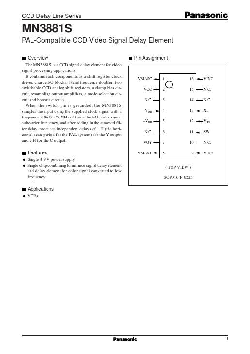
Pin Assignment
VBIASC VOC N.
 MN3881S Datasheet