Datasheet Details
| Part number | TSSOP48 |
|---|---|
| Manufacturer | Philips |
| File Size | 84.44 KB |
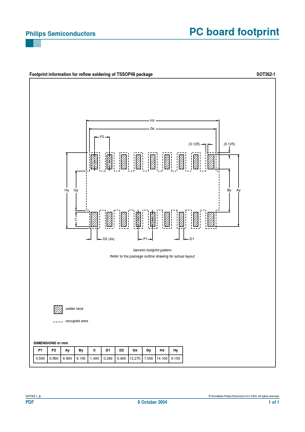
| Description | PC board footprint |
| Datasheet |
 TSSOP48-Philips.pdf TSSOP48-Philips.pdf
|
|
|
|
The TSSOP48 by Philips is a PC board footprint. Below is the official datasheet preview.
| Part number | TSSOP48 |
|---|---|
| Manufacturer | Philips |
| File Size | 84.44 KB |
| Description | PC board footprint |
| Datasheet |
TSSOP48-Philips.pdf
|
|
|
|
📁 TSSOP48 Similar Datasheet