HD74AC673 Datasheet, Register, Renesas Technology

PDF File Details

Part number:

HD74AC673

Manufacturer:

Renesas ↗ Technology

File Size:

420.56kb

Download:

📄 Datasheet

Description:

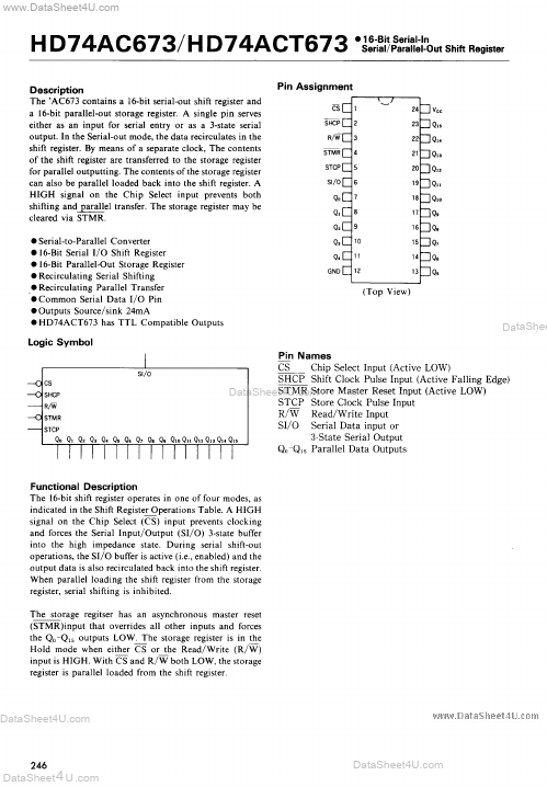
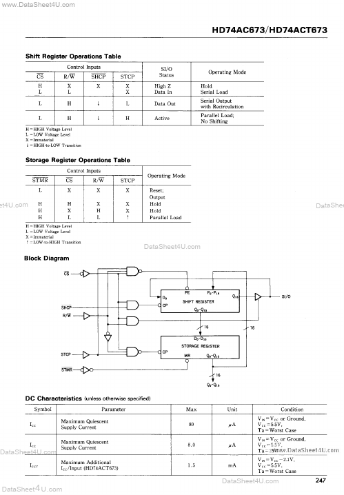
16-bit serial in serial / parallel out shift register.

Datasheet Preview: HD74AC673 📥 Download PDF (420.56kb)
Page 2 of HD74AC673 Page 3 of HD74AC673

TAGS

HD74AC673
16-Bit
Serial
Serial
Parallel
Out
Shift
Register
Renesas Technology

📁 Related Datasheet

HD74AC670 - 4 x 4 Register File with 3-State Output (Hitachi Semiconductor)
.

HD74AC670 - 4 x 4 Register File (Renesas Technology)
.. DataShee . . . DataSheet 4 U . .. et4U. DataShee DataShee.

HD74AC674 - 16-Bit Serial / Parallel in Serial Out Shift Register (Renesas Technology)
.. DataShee . . . DataSheet 4 U . .. et4U. DataShee DataShee.

HD74AC00 - Quad 2-Input NAND Gate (Hitachi Semiconductor)
HD74AC00 Quad 2-Input NAND Gate Feature • Outputs Source/Sink 24 mA Pin Arrangement 1 2 3 4 5 6 GND 7 (Top view) 14 VCC 13 12 11 10 9 8 DC Charac.

HD74AC00 - Quad 2-Input NAND Gate (Renesas)
HD74AC00 Quad 2-Input NAND Gate Features • Outputs Source/Sink 24 mA REJ03D0239–0200Z (Previous ADE-205-355 (Z)) Rev.2.00 Jul.16.2004 • Ordering In.

HD74AC02 - Quad 2-Input NOR Gate (Hitachi Semiconductor)
HD74AC02 Quad 2-Input NOR Gate Feature • Outputs Source/Sink 24 mA Pin Arrangement 1 2 3 4 5 6 GND 7 (Top view) 14 VCC 13 12 11 10 9 8 DC Charact.

HD74AC02 - Quad 2-Input NAND Gate (Renesas)
HD74AC02 Quad 2-Input NAND Gate Features • Outputs Source/Sink 24 mA REJ03D0240–0200Z (Previous ADE-205-356 (Z)) Rev.2.00 Jul.16.2004 • Ordering In.

HD74AC04 - Hex Inverter (Hitachi Semiconductor)
HD74AC04 Hex Inverter Feature • Outputs Source/Sink 24 mA Pin Arrangement 1 2 3 4 5 6 GND 7 (Top view) 14 VCC 13 12 11 10 9 8 DC Characteristics .

HD74AC04 - Hex Inverter (Renesas)
HD74AC04 Hex Inverter Features • Outputs Source/Sink 24 mA REJ03D0241–0200Z (Previous ADE-205-357 (Z)) Rev.2.00 Jul.16.2004 • Ordering Information .

HD74AC08 - Quad 2-Input AND Gate (Hitachi Semiconductor)
HD74AC08 Quad 2-Input AND Gate Feature • Outputs Source/Sink 24 mA Pin Arrangement 1 2 3 4 5 6 GND 7 (Top view) 14 VCC 13 12 11 10 9 8 DC Charact.

Since 2006. D4U Semicon.   |   Datasheet4U.com   |   Contact Us   |   Privacy Policy   |   Purchase of parts