Datasheet Details
- Part number
- ICS98UAE877A
- Manufacturer
- Renesas ↗
- File Size
- 403.20 KB
- Datasheet
- ICS98UAE877A-Renesas.pdf
- Description
- 1.5V LOW-POWER WIDE-RANGE FREQUENCY CLOCK DRIVER
ICS98UAE877A Description
DATASHEET 1.5V LOW-POWER WIDE-RANGE FREQUENCY CLOCK DRIVER ICS98UAE877A .
The PLL clock buffer, ICS98UAE877A, is designed for a VDDQ of 1.
ICS98UAE877A Features
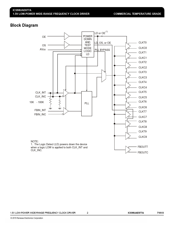
* Low skew, low jitter PLL clock driver
* 1 to 10 differential clock distribution
* Feedback pins for input to output synchronization
* Spread Spectrum tolerant inputs
* Auto PD when input signal is at a certain logic state
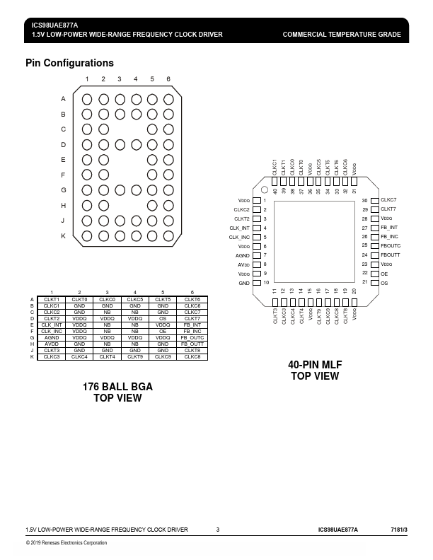
* Available in 52-ball VFBGA
ICS98UAE877A Applications
* DDR2 Memory Modules / Zero Delay Board Fan Out
* Provides complete DDR DIMM solution with
IDT74SSTUAE32xxx family
Switching Characteristics
* Period jitter:
40ps (DDR2-400/533) 30ps (DDR2-667)
* Half-period jitter:
60ps (DDR2-400/533) 50ps (DDR2-667)
📁 Related Datasheet
📌 All Tags
ICS98UAE877A Stock/Price