Datasheet Details
- Part number
- K7P321866M
- Manufacturer
- Samsung semiconductor
- File Size
- 477.32 KB
- Datasheet
- K7P321866M_Samsungsemiconductor.pdf
- Description
- 1Mx36 & 2Mx18 SRAM
K7P321866M Description
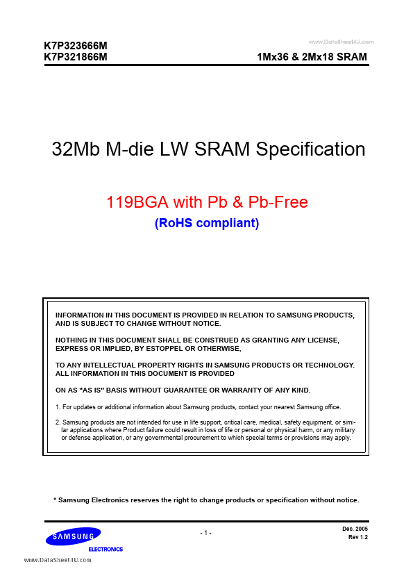
K7P323666M K7P321866M www.DataSheet4U.com 1Mx36 & 2Mx18 SRAM 32Mb M-die LW SRAM Specification 119BGA with Pb & Pb-Free (RoHS compliant) INFORMATIO.
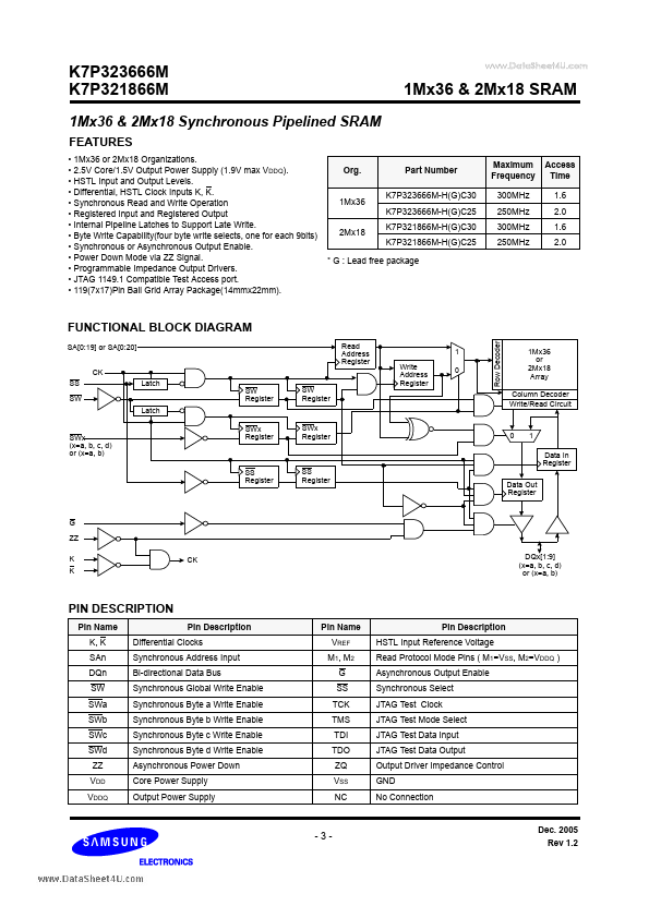
Pin Name K, K SAn DQn SW SWa SWb SWc SWd ZZ VDD VDDQ Pin Description Differential Clocks Synchronous Address Input Bi-directional Data Bus Synchronous.
K7P321866M Features
* 1Mx36 or 2Mx18 Organizations.
* 2.5V Core/1.5V Output Power Supply (1.9V max VDDQ).
* HSTL Input and Output Levels.
* Differential, HSTL Clock Inputs K, K.
* Synchronous Read and Write Operation
* Registered Input and Registered Output
* Inte
K7P321866M Applications
* where Product failure could result in loss of life or personal or physical harm, or any military or defense application, or any governmental procurement to which special terms or provisions may apply.
* Samsung Electronics reserves the right to change products or specification without notice.
📁 Related Datasheet
📌 All Tags
K7P321866M Stock/Price