Datasheet Details
- Part number
- K7P401823B, K7P403623B
- Manufacturer
- Samsung semiconductor
- File Size
- 344.45 KB
- Datasheet
- K7P403623B_Samsungsemiconductor.pdf
- Description
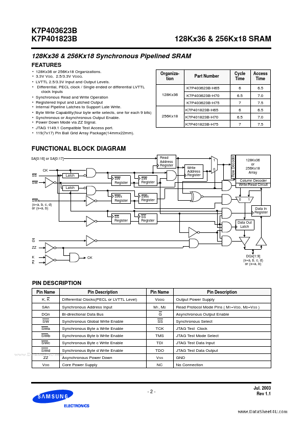
- 128Kx36 & 256Kx18 SRAM
- Note
- This datasheet PDF includes multiple part numbers: K7P401823B, K7P403623B.
Please refer to the document for exact specifications by model.