Datasheet Details
| Part number | LC8900KQ |
|---|---|
| Manufacturer | Sanyo |
| File Size | 146.15 KB |
| Description | Digital Audio Interface Receiver |
| Datasheet |
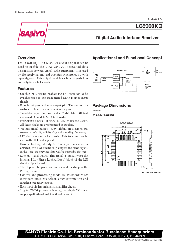
 LC8900KQ Datasheet LC8900KQ Datasheet
|
|
|
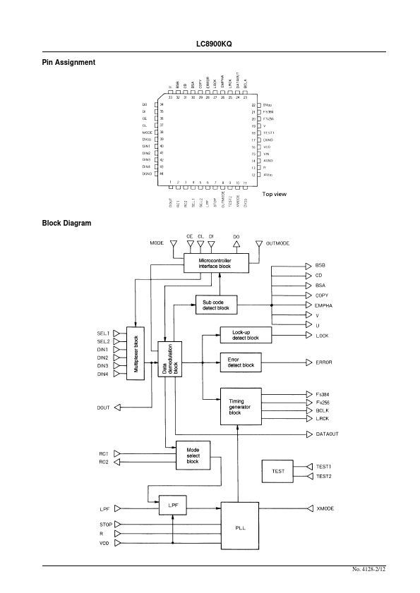
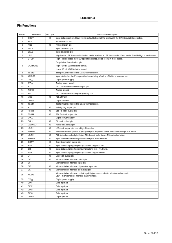
Input data output pin.
However, its output is fixed at the low level if the DIN4 input pin is selected.
RC oscillation pin RC oscillation pin Input pin select pin Input pin select pin High level = LPF time constant select mode.
| Part number | LC8900KQ |
|---|---|
| Manufacturer | Sanyo |
| File Size | 146.15 KB |
| Description | Digital Audio Interface Receiver |
| Datasheet |
LC8900KQ Datasheet
|
|
|
|