Datasheet Details
| Part number | LC8991 |
|---|---|
| Manufacturer | Sanyo |
| File Size | 39.24 KB |
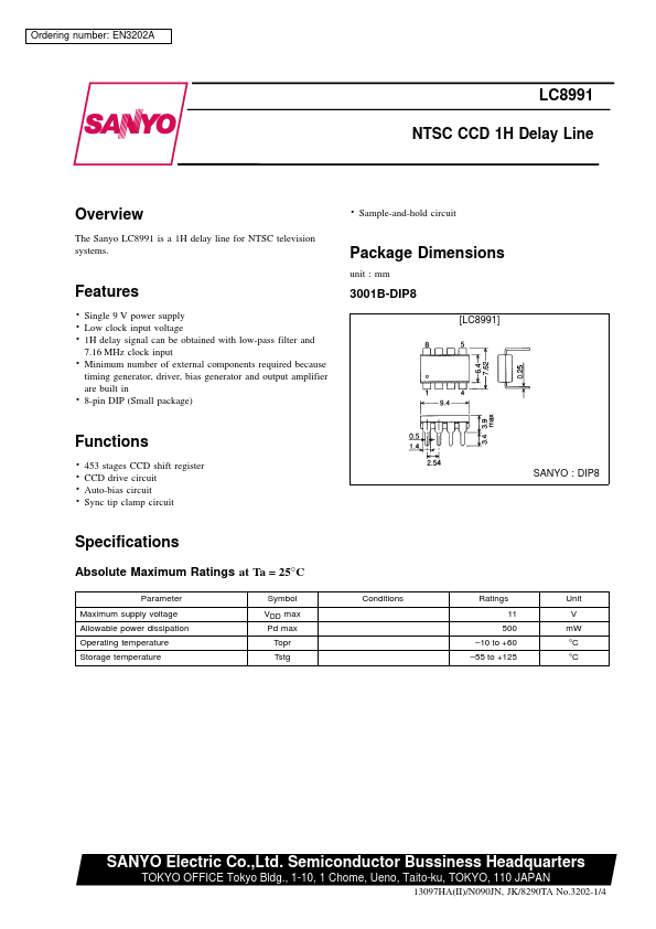
| Description | NTSC CCD 1H Delay Line |
| Datasheet |
 LC8991_SanyoSemiconDevice.pdf LC8991_SanyoSemiconDevice.pdf
|
| Part number | LC8991 |
|---|---|
| Manufacturer | Sanyo |
| File Size | 39.24 KB |
| Description | NTSC CCD 1H Delay Line |
| Datasheet |
LC8991_SanyoSemiconDevice.pdf
|
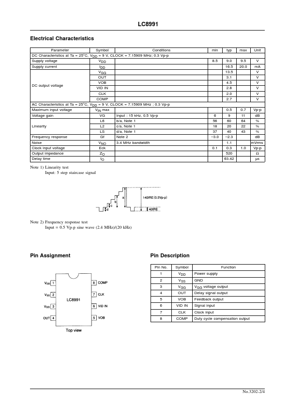
Pin No.
📁 LC8991 Similar Datasheet