Datasheet Details
- Part number
- LC89975M
- Manufacturer
- Sanyo
- File Size
- 98.25 KB
- Datasheet
- LC89975M_SanyoSemiconDevice.pdf
- Description
- PAL-Format Delay Line
LC89975M Description
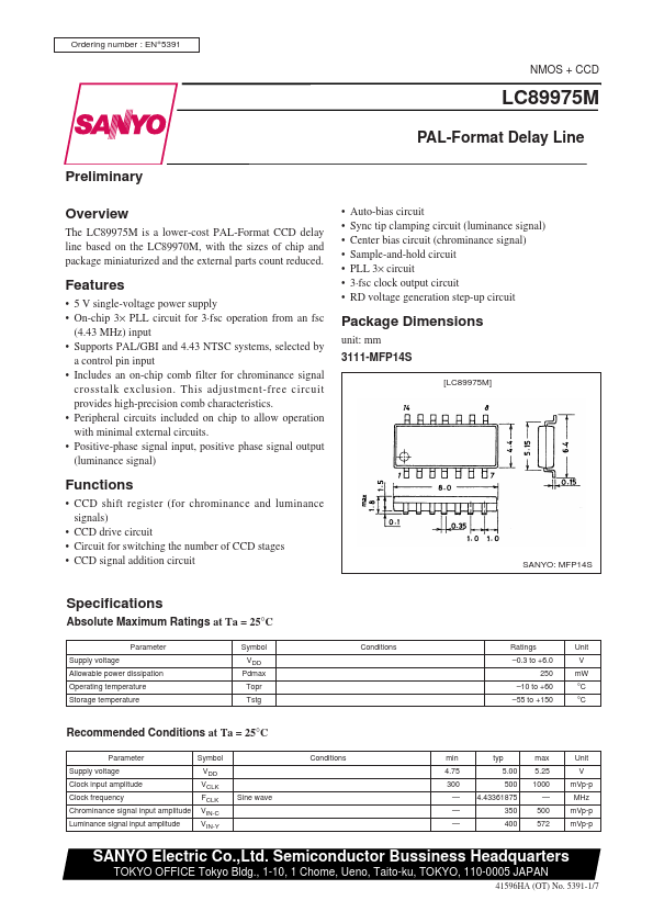
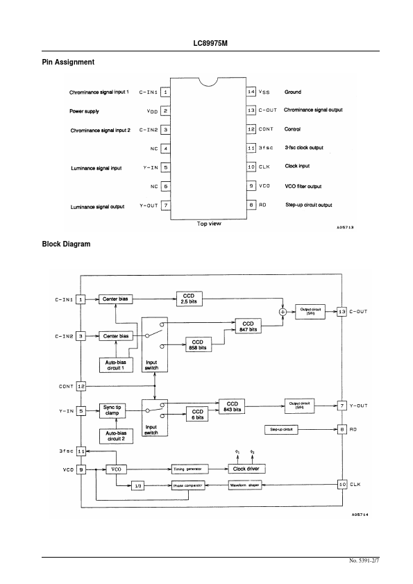
Ordering number : EN *5391 NMOS + CCD LC89975M PAL-Format Delay Line Preliminary Overview The LC89975M is a lower-cost PAL-Format CCD delay line .
LC89975M Features
* 5 V single-voltage power supply
* On-chip 3× PLL circuit for 3
* fsc operation from an fsc (4.43 MHz) input
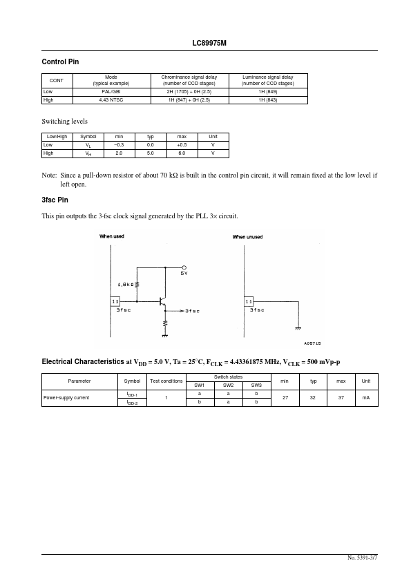
* Supports PAL/GBI and 4.43 NTSC systems, selected by a control pin input
* Includes an on-chip comb filter for chrominance signal crosstalk exclusion. This
📁 Related Datasheet
📌 All Tags