Description
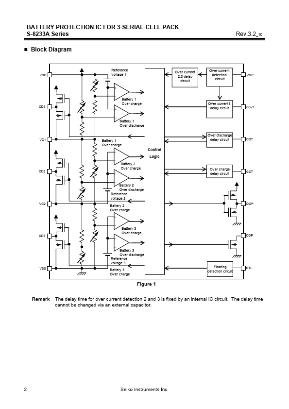
1 DOP Connects FET gate for discharge control (CMOS output) 2 COP Connects FET gate for charge control (Nch open-drain output) 3 VMP Detects voltage between VCC to VMP(Over current detection pin) 4 COVT Connects capacitor for over current detection1delay circuit 5 CDT Connects capacitor for over discharge detection delay circuit 6 CCT Connects capacitor for over charge detection delay circuit 7 VSS Negative power input, and connects negative voltage for battery 3 8 CTL Charge/discharge control s
Features
- (1) Internal high-accuracy voltage detection circuit Over charge detection voltage 4.10 ± 0.05 V to 4.35 ± 0.05 V 50 mV- step Over charge release voltage 3.85 ± 0.10 V to 4.35 ± 0.10 V 50 mV- step (The over charge release voltage can be selected within the range where a difference from over charge detection voltage is 0 V to 0.3 V) Over discharge detection voltage 2.00 ± 0.08 V to 2.70± 0.08 V 100 mV- step Over discharge release voltage 2.00 ± 0.10 V to 3.70± 0.10 V 100 mV - step (The over disch.
 S82-33A.pdf