Description
Connects FET gate for discharge control (CMOS output) Non connect
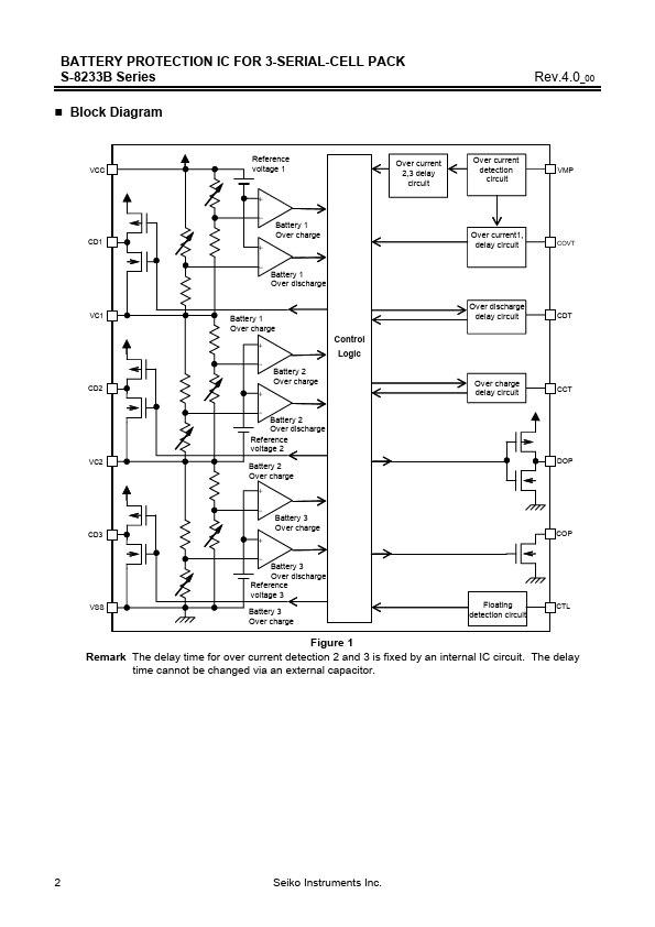
Connects FET gate for charge control (Nch open-drain output) Detects voltage between VCC to VMP(Over current detection pin) Connects capacitor for over current detection1delay circuit Connects capacitor for over discharge detection delay circuit Connects capacitor for over charge detection delay circuit Negative power input, and connects negative voltage for battery 3 Charge/discharge control signal input Battery 3 conditioning s
Features
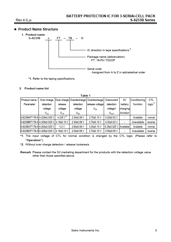
- (1) Internal high-accuracy voltage detection circuit Over charge detection voltage 3.80 ± 0.025 V to 4.40 ± 0.025 V 5 mV - step Over charge release voltage 3.45 ± 0.100 V to 4.40 ± 0.100 V 5 mV - step (The over charge release voltage can be selected within the range where a difference from over charge detection voltage is 0 to 0.35 V with 50 mV - step) Over discharge detection voltage 2.00 ± 0.08 V to 2.80± 0.08 V 50 mV - step Over discharge release voltage 2.00 ± 0.10 V to4.00± 0.10 V 50 mV - s.
 S82-33B.pdf