Datasheet Details
| Part number | TC59YM916BKG24A |
|---|---|
| Manufacturer | Toshiba ↗ America Electronic |
| File Size | 1.37 MB |
| Description | 512-megabit XDRTM DRAM The Rambus XDRTM DRAM device |
| Datasheet |
 TC59YM916BKG24A_ToshibaAmericaElectronic.pdf TC59YM916BKG24A_ToshibaAmericaElectronic.pdf
|
| Part number | TC59YM916BKG24A |
|---|---|
| Manufacturer | Toshiba ↗ America Electronic |
| File Size | 1.37 MB |
| Description | 512-megabit XDRTM DRAM The Rambus XDRTM DRAM device |
| Datasheet |
TC59YM916BKG24A_ToshibaAmericaElectronic.pdf
|
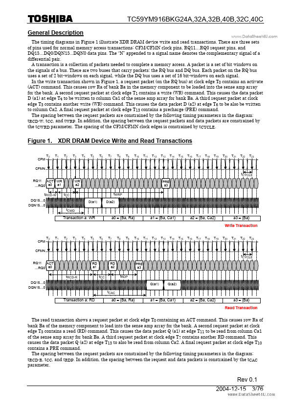
www.DataSheet4U.com The timing diagrams in Figure 1 illustrate XDR DRAM device write and read transactions.There are three sets of pins used for normal memory access transactions: CFM/CFMN clock pins, RQ11…RQ0 request pins, and DQ15…DQ0/DQN15DQN0 data pins.The “N” appended to a signal name denotes the complementary signal of a differential pair.A transaction is a collection of packets needed to complete a memory access.A packet is a set of bit windows on the signals of a bus.There are two
📁 TC59YM916BKG24A Similar Datasheet