Datasheet Details
| Part number | 74LVC3G16 |
|---|---|
| Manufacturer | nexperia |
| File Size | 212.09 KB |
| Description | Triple buffer |
| Datasheet |
 74LVC3G16 Datasheet 74LVC3G16 Datasheet
|
|
|
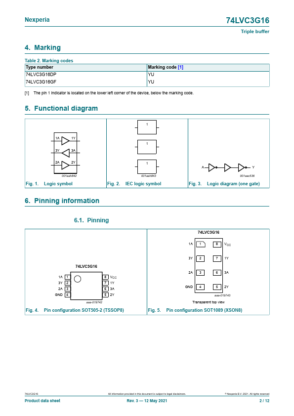
The 74LVC3G16 provides three buffers.
The inputs can be driven from either 3.3 V or 5 V devices.
This feature allows the use of the 74LVC3G16 as a translator in a mixed 3.3 V and 5 V environment.
| Part number | 74LVC3G16 |
|---|---|
| Manufacturer | nexperia |
| File Size | 212.09 KB |
| Description | Triple buffer |
| Datasheet |
74LVC3G16 Datasheet
|
|
|
|