Datasheet Details
| Part number | 74LVC3G34-Q100 |
|---|---|
| Manufacturer | nexperia |
| File Size | 206.37 KB |
| Description | Triple buffer |
| Datasheet |
 74LVC3G34-Q100 Datasheet 74LVC3G34-Q100 Datasheet
|
|
|
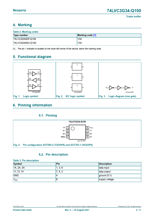
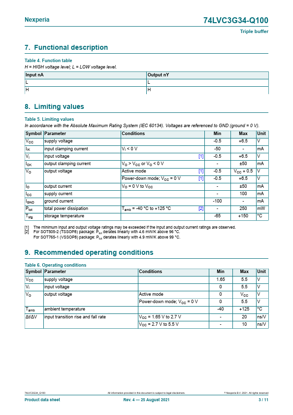
The 74LVC3G34-Q100 is a triple buffer.
Inputs can be driven from either 3.3 V or 5 V devices.
This feature allows the use of these devices as translators in mixed 3.3 V and 5 V environments.
| Part number | 74LVC3G34-Q100 |
|---|---|
| Manufacturer | nexperia |
| File Size | 206.37 KB |
| Description | Triple buffer |
| Datasheet |
74LVC3G34-Q100 Datasheet
|
|
|
|