Datasheet4U Logo Datasheet4U.com

ACE7401B - P-Channel Enhancement Mode Field Effect Transistor

Description

The ACE7401B uses advanced trench technology to provide excellent RDS(ON), and ultra-low low gate charge with a 25V gate rating.

This device is suitable for use as a load switch or in PWM applications.

Features

  • VDS(V)=-30V.
  • ID=-29A (VGS=-10V).
  • RDS(ON)<13mΩ (VGS=-20V).
  • RDS(ON)<14mΩ (VGS=-10V).
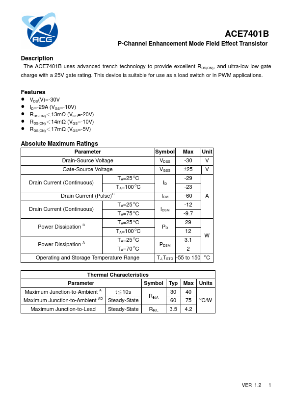
  • RDS(ON)<17mΩ (VGS=-5V) Absolute Maximum Ratings Parameter Drain-Source Voltage Gate-Source Voltage Drain Current (Continuous) TA=25 OC TA=100 OC Drain Current (Pulse)C Drain Current (Continuous) TA=25 OC TA=75 OC Power Dissipation B TA=25 OC TA=100 OC Power Dissipation A TA=25 OC TA=70 OC Operating and Storage Temperature Range Symbol Max Unit VDSS -30 V VGSS ±25 V -29 ID.

📥 Download Datasheet

Datasheet preview – ACE7401B

Datasheet Details

Part number ACE7401B
Manufacturer ACE Technology
File Size 598.71 KB
Description P-Channel Enhancement Mode Field Effect Transistor
Datasheet download datasheet ACE7401B Datasheet
Additional preview pages of the ACE7401B datasheet.
Other Datasheets by ACE Technology

Full PDF Text Transcription

Click to expand full text
ACE7401B P-Channel Enhancement Mode Field Effect Transistor Description The ACE7401B uses advanced trench technology to provide excellent RDS(ON), and ultra-low low gate charge with a 25V gate rating. This device is suitable for use as a load switch or in PWM applications. Features  VDS(V)=-30V  ID=-29A (VGS=-10V)  RDS(ON)<13mΩ (VGS=-20V)  RDS(ON)<14mΩ (VGS=-10V)  RDS(ON)<17mΩ (VGS=-5V) Absolute Maximum Ratings Parameter Drain-Source Voltage Gate-Source Voltage Drain Current (Continuous) TA=25 OC TA=100 OC Drain Current (Pulse)C Drain Current (Continuous) TA=25 OC TA=75 OC Power Dissipation B TA=25 OC TA=100 OC Power Dissipation A TA=25 OC TA=70 OC Operating and Storage Temperature Range Symbol Max Unit VDSS -30 V VGSS ±25 V -29 ID -23 IDM -60 A -12 IDSM -9.
Published: |