AK8185A Description
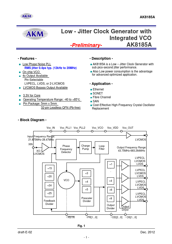
AK8185A is a Low Jitter Clock Generator with sub pico-second jitter performance. Also Low power consumption is the advantage for advanced optimized application. - Application Ethernet SONET Fibre Channel SAN Cost-Effective High-Frequency Crystal Oscillator Replacement - Block Diagram Vcc_IN Input Frequency Range:.
AK8185A Key Features
- Description AK8185A is a Low
- Jitter Clock Generator with sub pico-second jitter performance. Also Low power consumption is the advantage for advanced
- Application Ethernet SONET Fibre Channel SAN Cost-Effective High-Frequency Crystal Oscillator Replacement
- Block Diagram Vcc_IN Input Frequency Range: 21.875MHz-28.47MHz XIN XO / LVCMOS Phase Frequency Detector Charge Pump Loop
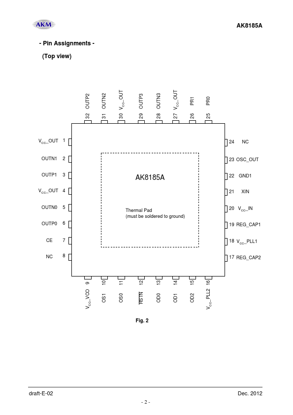
- Pin Assignments (Top view)