AK8186B Description
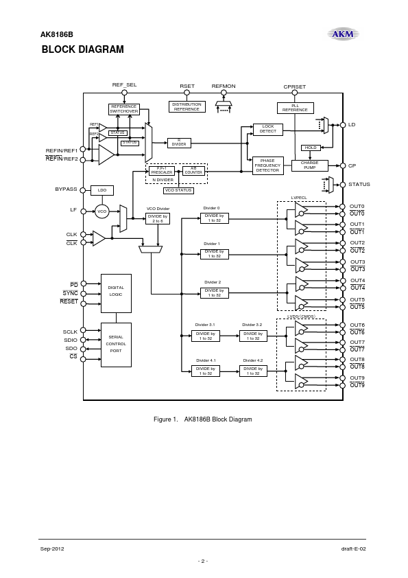
The AK8186B is a multi-output clock generator with sub-ps jitter performance. The on-chip VCO tunes from 1.75GHz to 2.25GHz. The distribution section has three pairs of LVPECL buffers (6 outputs) and two pairs of LVDS buffers (4 outputs)/eight CMOS buffers (two per LVDS outputs).
AK8186B Key Features
- 1 DESCRIPTION
- 1 ORDERING INFORMATION
- 1 BLOCK DIAGRAM
- 2 PIN DESCRIPTION