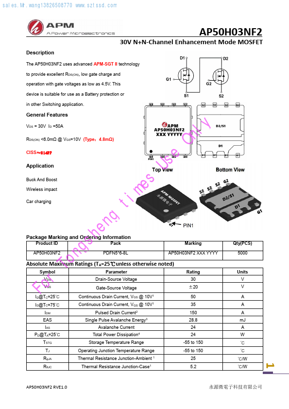
DESCRIPTION
AP50H03NF2 30V N+N-Channel Enhancement Mode MOSFET GENERAL FEATURES
VDS = 30V ID =50A RDS(ON) <6.0mΩ @ VGS=10V (Type:4.8mΩ) Only CISS≈814PF Application Use Buck And Boost Wireless impact Car charging times heng Package Marking and Ordering Information s Product ID Pack Marking g AP50H03NF2 PDFN5*6-8L AP50H03NF2 XXX YYYY Ton ABSOLUTE MAXIMUM RATINGS
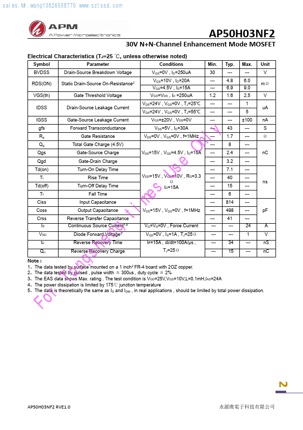
(TA=25℃unless otherwise noted) Symbol rVDS FoVGS Parameter Drain-Source Voltage Gate-Source Voltage Rating 30 ±20 ID@TC=25℃ Continuous Drain Current, VGS @ 10V1 50 ID@TC=75℃ IDM EAS Continuous Drain Current, VGS @ 10V1 Pulsed Drain Current2 Single Pulse Avalanche Energy3 35 150 28.8 IAS Avalanche Current 24 PD@TA=25℃ Total Power Dissipation4 24 TSTG Storage Temperature Range -55 to 150 TJ Operating Junction Temperature Range -55 to 150 RθJA Thermal Resistance Junction-Ambient 1 25 RθJC Thermal Resistance Junction-Case1 5.2 Qty(PCS) 5000 Units V V A A A mJ A W ℃ ℃ ℃/W ℃/W AP50H03NF2 RVE1.0 永源微電子科技有限公司 1 sales.Mr.wang13826508770 AP50H03NF2 30V N+N-Channel Enhancement Mode MOSFET ELECTRICAL CHARACTERISTICS
(TJ=25 ℃, unless otherwise noted) Symbol Parameter Conditions Min. APM