Datasheet Summary
July 2005 rev 0.2 3.3V 1:10 LVCMOS PLL Clock Generator
Features
- -
- Output frequency range: 25 MHz to 200 MHz Input frequency range: 6.25 MHz to 31.25 MHz 2.5V or 3.3V operation
The ASM5I9350 Features
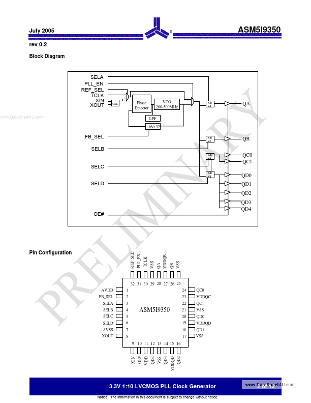
Xtal and LVCMOS reference clock inputs and provides nine outputs partitioned in four banks of 1, 1, 2, and 5 outputs. Bank A divides the VCO output by 2 or 4 while the other banks divide by 4 or 8 per SEL(A:D) settings, see Table 2. These dividers allow output to input ratios of 16:1, 8:1, 4:1, and 2:1. Each LVCMOS patible output can drive 50Ω series or parallel terminated transmission lines. For series terminated transmission lines, each output can drive one or two traces...