Datasheet4U Logo Datasheet4U.com

ASM5I9351 - 9-Output Zero Delay Buffer

Description

clock directly feeds the output dividers.

This mode is fully static and the minimum input clock frequency specification does not apply.

200MHz PLL-based zero delay buffer designed for high speed clock distribution applications.

Features

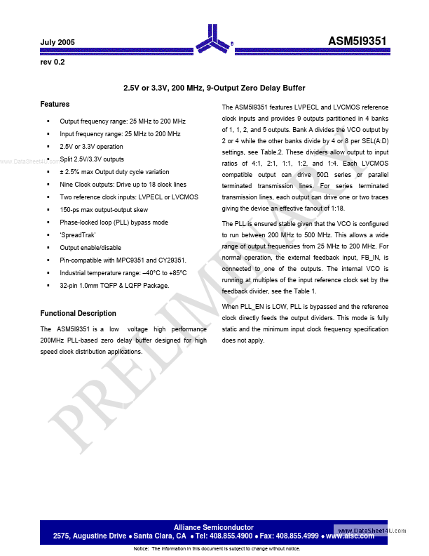
  • Output frequency range: 25 MHz to 200 MHz Input frequency range: 25 MHz to 200 MHz 2.5V or 3.3V operation ASM5I9351 The ASM5I9351 features LVPECL and LVCMOS reference clock inputs and provides 9 outputs partitioned in 4 banks of 1, 1, 2, and 5 outputs. Bank A divides the VCO output by 2 or 4 while the other banks divide by 4 or 8 per SEL(A:D) settings, see Table.2. These dividers allow output to input ratios of 4:1, 2:1, 1:1, 1:2, and 1:4. Each LVCMOS compatible output can dr.

📥 Download Datasheet

Datasheet preview – ASM5I9351

Datasheet Details

Part number ASM5I9351
Manufacturer Alliance Semiconductor
File Size 560.92 KB
Description 9-Output Zero Delay Buffer
Datasheet download datasheet ASM5I9351 Datasheet
Additional preview pages of the ASM5I9351 datasheet.
Other Datasheets by Alliance Semiconductor

Full PDF Text Transcription

Click to expand full text
July 2005 rev 0.2 2.5V or 3.3V, 200 MHz, 9-Output Zero Delay Buffer Features ƒ ƒ ƒ Output frequency range: 25 MHz to 200 MHz Input frequency range: 25 MHz to 200 MHz 2.5V or 3.3V operation ASM5I9351 The ASM5I9351 features LVPECL and LVCMOS reference clock inputs and provides 9 outputs partitioned in 4 banks of 1, 1, 2, and 5 outputs. Bank A divides the VCO output by 2 or 4 while the other banks divide by 4 or 8 per SEL(A:D) settings, see Table.2. These dividers allow output to input ratios of 4:1, 2:1, 1:1, 1:2, and 1:4. Each LVCMOS compatible output can drive 50Ω series or parallel terminated transmission lines. For series terminated transmission lines, each output can drive one or two traces giving the device an effective fanout of 1:18.
Published: |