ASM5I961C
ASM5I961C is Low Voltage Zero Delay Buffer manufactured by Alliance Semiconductor.
July 2005 rev 0.2 Low Voltage Zero Delay Buffer
Features
- -
- - Fully Integrated PLL Up to 200MHz I/O Frequency LVCMOS Outputs Outputs Disable in High Impedance
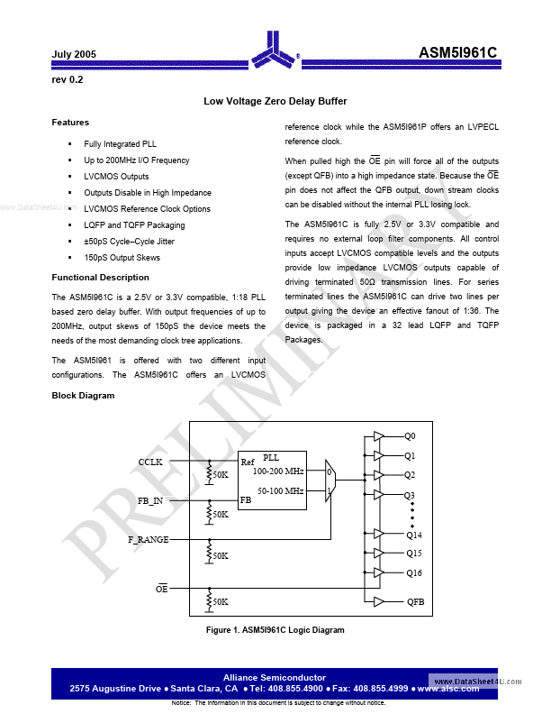
ASM5I961C reference clock while the ASM5I961P offers an LVPECL reference clock. When pulled high the OE pin will force all of the outputs (except QFB) into a high impedance state. Because the OE pin does not affect the QFB output, down stream clocks can be disabled without the internal PLL losing lock. The ASM5I961C is fully 2.5V or 3.3V patible and requires no external loop filter ponents. All control inputs accept LVCMOS patible levels and the outputs provide low impedance LVCMOS outputs capable of driving terminated...