FEATURES
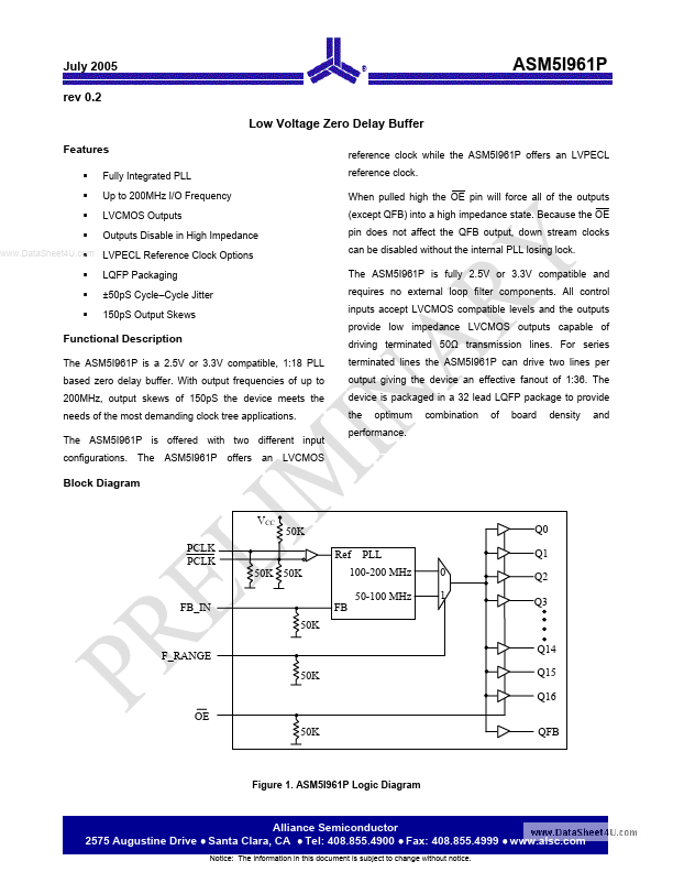
Fully Integrated PLL Up to 200MHz I/O Frequency LVCMOS Outputs Outputs Disable in High Impedance ASM5I961P reference clock while the ASM5I961P offers an LVPECL reference clock. Because the OE pin does not affect the QFB output, down stream clocks can be disabled without the internal PLL losing lock. All control inputs accept LVCMOS compatible levels and the outputs provide low impedance LVCMOS outputs capable of driving terminated 50Ω transmission lines. For series terminated lines the ASM5I961P can drive two lines per output giving the device an effective fanout of 1:36. The device is packaged in a 32 lead LQFP package to provide the optimum combination of board density and performance. LVPECL Reference Clock Options LQFP Packaging ±50pS Cycle–Cycle Jitter 150pS Output Skews Functional DESCRIPTION
The ASM5I961P is a 2.5V or 3.3V compatible, 1:18 PLL based zero delay buffer. With output frequencies of up to 200MHz, output skews of 150pS the device meets the needs of the most demanding clock tree applications. Alliance Semiconductor