The following content is an automatically extracted verbatim text
from the original manufacturer datasheet and is provided for reference purposes only.
View original datasheet text
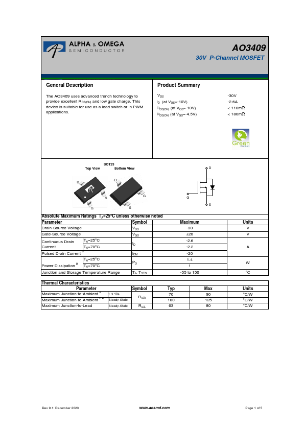
AO3409
30V P-Channel MOSFET
General Description
The AO3409 uses advanced trench technology to provide excellent RDS(ON) and low gate charge. This device is suitable for use as a load switch or in PWM applications.
Product Summary
VDS ID (at VGS=-10V) RDS(ON) (at VGS=-10V) RDS(ON) (at VGS=-4.5V)
-30V -2.6A < 110mW < 180mW
SOT23
Top View
Bottom View
D
D D
S
G
G
S
Absolute Maximum Ratings TA=25°C unless otherwise noted
Parameter
Symbol
Drain-Source Voltage
VDS
Gate-Source Voltage
VGS
Continuous Drain Current
TA=25°C TA=70°C
ID
Pulsed Drain Current C
IDM
TA=25°C Power Dissipation B TA=70°C
PD
Junction and Storage Temperature Range
TJ, TSTG
G S
Maximum -30 ±20 -2.6 -2.2 -20 1.
 AO3409 Datasheet